Gate-enhanced junction varactor with gradual capacitance variation

a varactor and capacitance variation technology, applied in the field of varactors, can solve the problems of complex process for manufacturing components of integrated circuits, complicated process, etc., and achieve the effect of facilitating the control of varactor capacitance and high maximum-to-minimum varactor capacitance ratio

Inactive Publication Date: 2006-07-25
NAT SEMICON CORP
View PDF16 Cites 28 Cited by
  • Summary
  • Abstract
  • Description
  • Claims
  • Application Information

AI Technical Summary

Benefits of technology

[0036]The present invention furnishes a variation, or extension, of the gate-enhanced junction varactor of U.S. application Ser. No. 09 / 903,059. The varactor capacitance in the present gate-enhanced semiconductor junction varactor normally changes in a relatively gradual manner, compared to that of U.S. application Ser. No. 09 / 903,059, as the plate-to-body voltage is varied across substantially its entire voltage range at a suitable fixed value of the gate-to-body voltage. This facilitates controlling the varactor capacitance in the present invention.
[0040]The gate-to-body voltage is controlled in such a way that an inversion layer forms in the surface depletion region at a certain value of the plate-to-body voltage. The inversion layer meets the plate region. By adjusting the plate-to-body voltage in a specified (positive or negative) manner, the inversion layer disappears laterally in stages such that any inversion-layer material remaining after each disappearing stage meets the plate region. That is, the inversion layer shrinks laterally in stages toward the plate region. One portion of the inversion layer disappears followed by another portion until all of the inversion layer is gone. The net effect is that the inversion layer gradually disappears as the plate-to-body voltage is appropriately adjusted.
[0042]Upon adjusting the plate-to-body voltage so as to cause a portion of the inversion layer to disappear, the second capacitor plate shrinks laterally. The second capacitor plate is then formed by the remainder of the inversion layer and the undepleted material of the plate region since the remainder of the inversion layer meets the plate region. The lateral shrinkage of the second capacitor plate reduces its area, thereby reducing the varactor capacitance.

Problems solved by technology

However, improving the capacitance ratio in this way necessitates an additional masked ion implantation into the varactor area and complicates the process for manufacturing an integrated circuit containing components other than the varactor.
Switched-capacitor varactors require switching control and thus are also relatively complex.

Method used


Image

  • Gate-enhanced junction varactor with gradual capacitance variation
  • Gate-enhanced junction varactor with gradual capacitance variation
  • Gate-enhanced junction varactor with gradual capacitance variation

Examples


Embodiment Construction

General Considerations

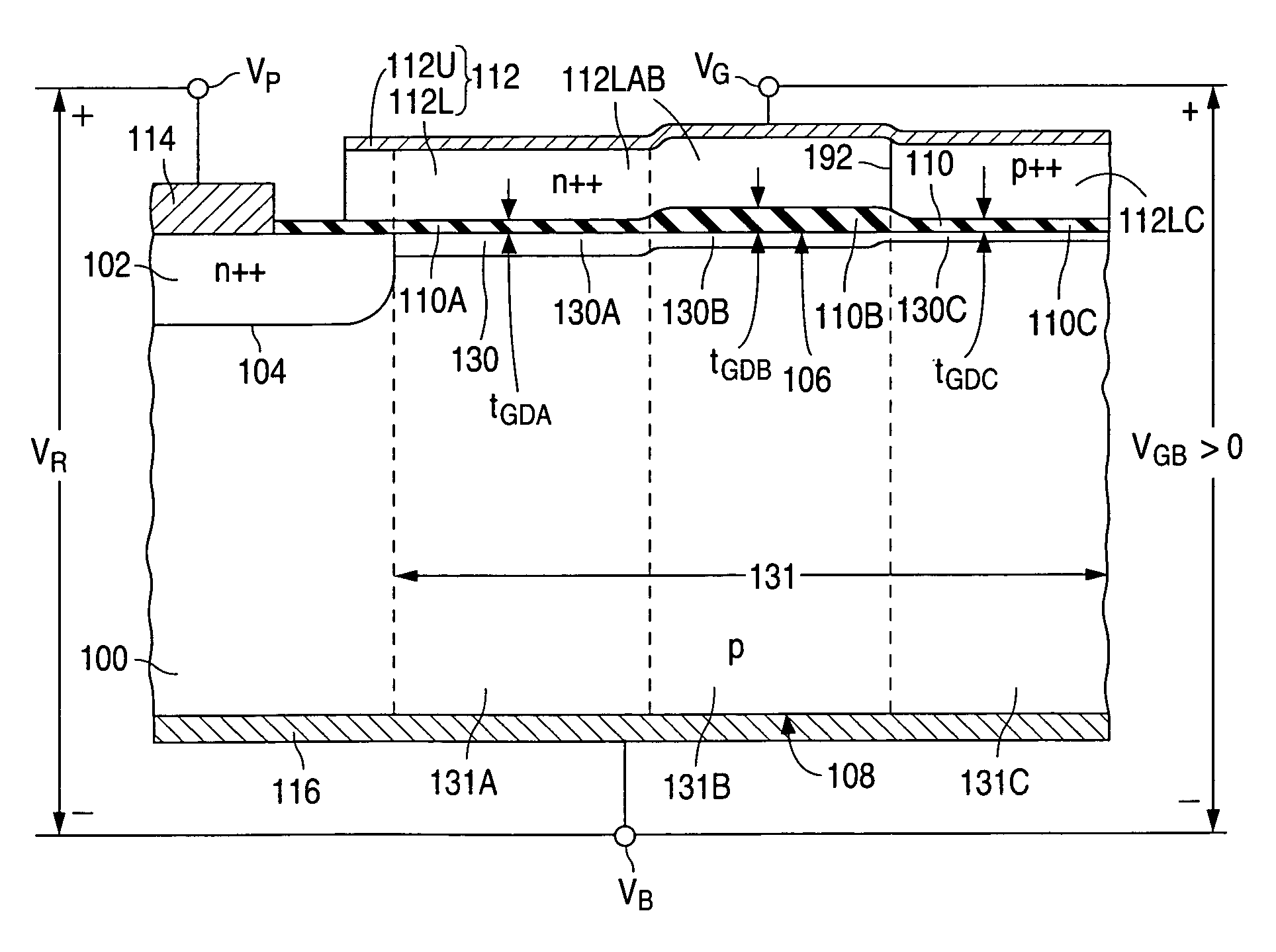
[0083]The term “n-channel” as used here in describing a gate-enhanced junction varactor means that the varactor has a surface charge-inversion layer (or channel) in which the charge carriers are electrons. The term “p-channel” as used here in describing a gate-enhanced junction varactor similarly means that the varactor has a surface charge-inversion layer (or channel) in which the charge carriers are holes.

[0084]An electrical signal, such as a voltage (or electrical potential), generally consists of a direct-current (“DC”) signal and / or an AC signal which varies with time at a frequency that may itself vary with time. The DC signal may vary with time. Any time variation of the DC signal is either not at a significant identifiable frequency or is at a frequency much lower than that of the AC signal. A bias signal, such as a bias voltage, is a DC signal employed to place parts of an electronic circuit, including a single circuit element, in a specified bias (e.g...


PUM


Abstract

A semiconductor junction varactor utilizes gate enhancement for enabling the varactor to achieve a high ratio of maximum capacitance to minimum capacitance. The varactor has a gate region (131 or 181) divided into multiple portions of differing zero-point threshold voltages for enabling the varactor capacitance to vary relatively gradually with a control voltage applied to the varactor.

Description

FIELD OF USE[0001]This invention relates to varactors. More particularly, this invention relates to varactors provided in, and / or utilized with, semiconductor integrated circuits.BACKGROUND ART[0002]A varactor is a variable capacitor, i.e., a capacitor whose capacitance can be changed as a function of one or more control signals. The term “varactor” is derived from “variable” and “reactor”, and means a device whose reactance can be varied in a controlled manner. The term “varicap”, derived from “variable” and “capacitor”, is also used to describe such a device.[0003]Varactors are employed in various parts of electronic systems. For example, varactors are utilized in voltage-controlled oscillators (“VCOs”) of wireless communications systems. A VCO generates a local oscillator signal for use in performing heterodyne frequency conversion in transceiver circuitry of a wireless communication system. The frequency of the oscillator signal changes as a function of a control voltage. In a V...

Claims


Application Information

Patent Timeline
Patent Type & Authority Patents(United States)
IPC IPC(8): H01L29/93H01L27/08H03B5/12
CPCH01L27/0808H03B5/1243H03B5/1215H03B5/1228
Inventor BULUCEA, CONSTANTIN
Owner NAT SEMICON CORP
Why Eureka
Try Eureka