Thin film shape memory alloy actuated microrelay

a micro-relay and memory alloy technology, applied in relays, generators/motors, contact mechanisms, etc., can solve the problems of power consumption and difficulty in small-scale manufacturing, and achieve the effect of relatively large current, low manufacturing cost and low cos

Inactive Publication Date: 2006-08-01
TINI ALLOY
View PDF4 Cites 29 Cited by
  • Summary
  • Abstract
  • Description
  • Claims
  • Application Information

AI Technical Summary

Benefits of technology

[0012]Other objects of the invention are to make a microrelay that can be microfabricated in arrays, which latches so that power is not consumed most of the time, has near zero insertion loss, conducts relatively large current, and can be manufactured inexpensively in large volume.
[0014]Another object is to provide MEMS microrelays which can give engineers and designers a new cost-effective option for use in telecommunications, aerospace automated test equipment, and other applications in various emerging markets.
[0015]Another object is to provide MEMS microrelays which can be batch fabricated on a silicon wafer using MEMS technology, thus making them mass producible and inexpensive.

Problems solved by technology

Relays usually are operated by electromagnetic solenoids: these are difficult to manufacture in very small size.
The disadvantage is that a voltage drop occurs across the component such that it consumes power even when inactive.

Method used


Image

  • Thin film shape memory alloy actuated microrelay
  • Thin film shape memory alloy actuated microrelay
  • Thin film shape memory alloy actuated microrelay

Examples


Embodiment Construction

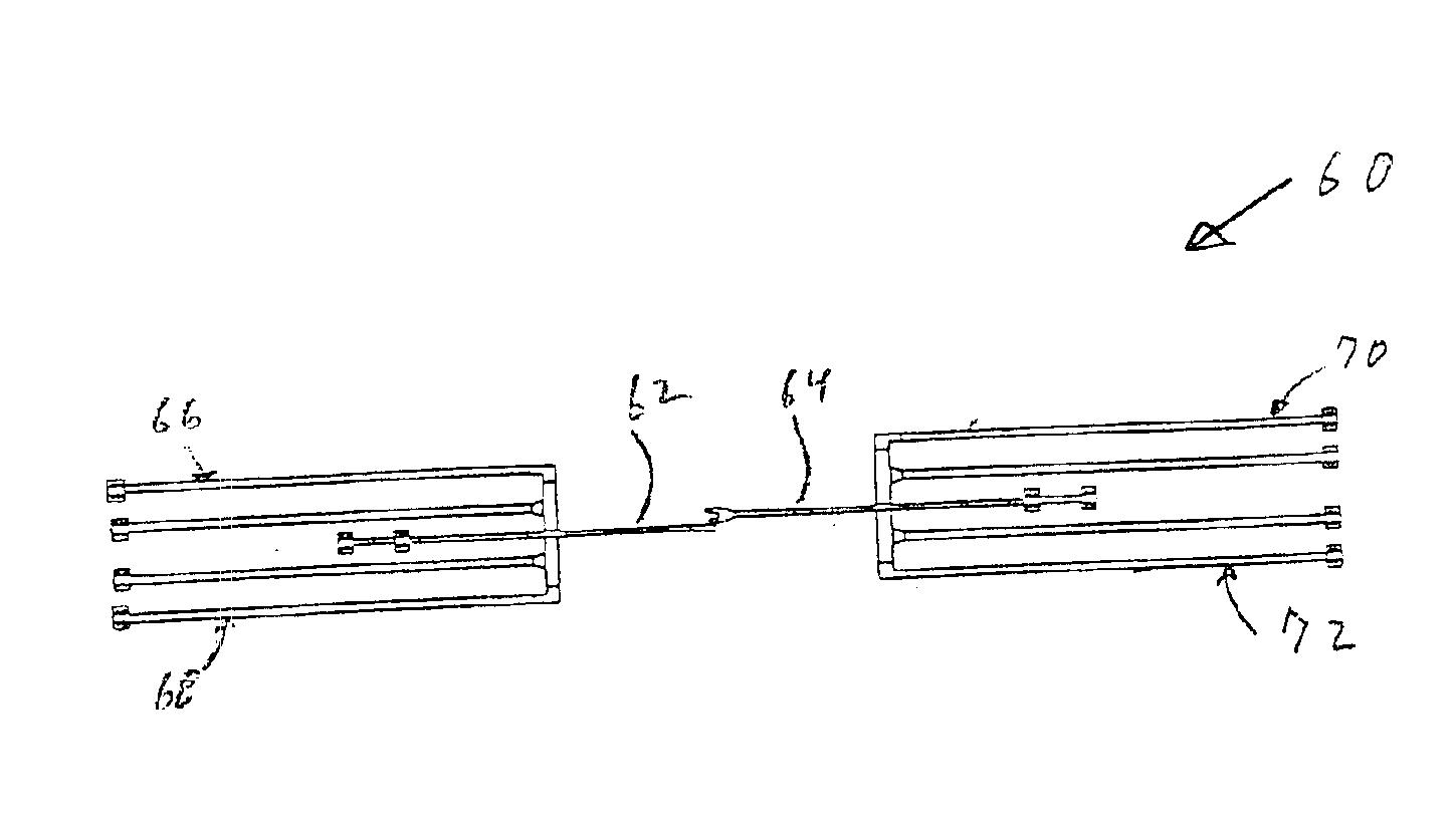
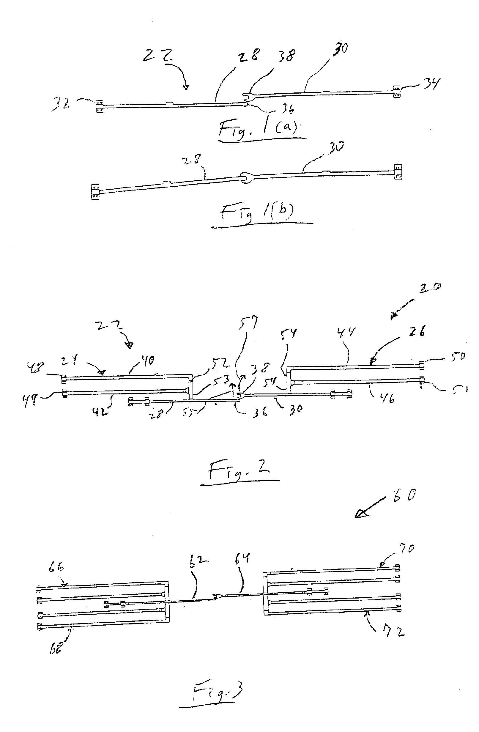
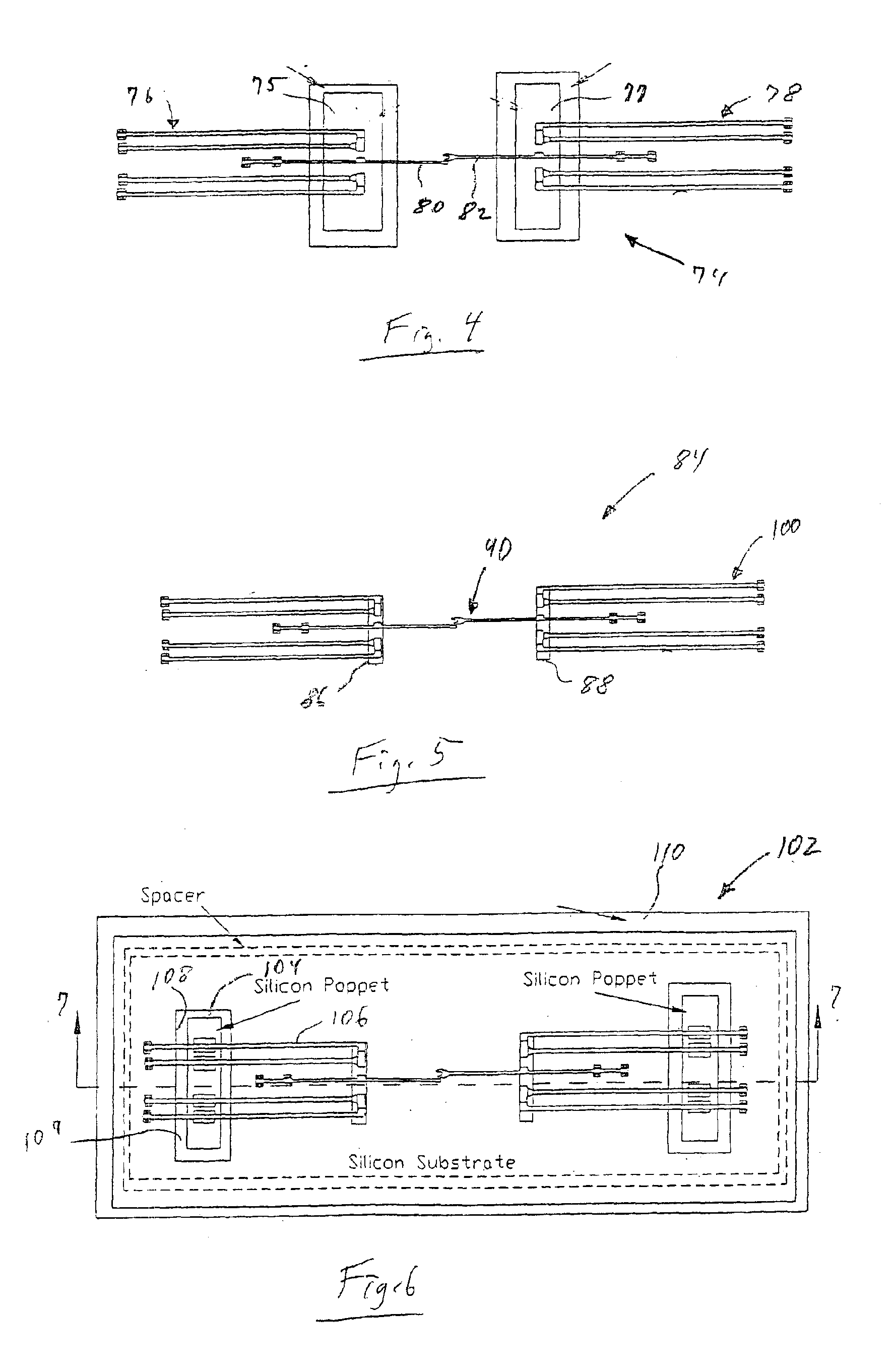
[0032]In its general concept, the invention comprises a thin film device 20 in which microrelay 22 of FIGS. 1(a) and 1(b) is in combination with shape memory alloy (SMA) actuators 24 and 26 of FIG. 2. The microrelay / actuator device 20 achieves the advantages of high work output per unit mass, small size, rapid actuation, higher efficiency than differential thermal expansion, good impedance match (operates at TTL level voltages), purely resistive impedance (no magnetic coil), and which can be fabricated using MEMS technology.

[0033]In the invention microfabrication techniques used for the fabrication of microelectro-mechanical systems (MEMS) coupled with sputter deposited thin film SMA actuation technology enable the mass production of device arrays with high current carrying microrelays. The SMA material can be made in thin film configurations in accordance with the teachings of U.S. Pat. No. 5,061,914 to Busch et. al. for Shape Memory Alloy Microactuator, the disclosure of which is ...


PUM


Abstract

A microrelay device formed on a silicon substrate wafer for use in opening and closing a current path in a circuit. A pair of electrically conducting latching beams are attached at their proximal ends to terminals on the substrate. Proximal ends of the beams have complementary shapes which releasably fit together to latch the beams and close the circuit. A pair of shape memory alloy actuators are selectively operated to change shapes which bend one of the beams in a direction which latches the distal ends, or bend the other beam to release the distal ends and open the circuit. The microrelay is bistable in its two positions, and power to the actuators is applied only for switching it open or closed.

Description

CROSS-REFERENCE TO PRIOR APPLICATIONS[0001]This application claims the benefit under 35 USC §119(e) of U.S. provisional application Ser. No. 60 / 192,766 filed Mar. 28, 2000 and is a divisional of application Ser. No. 09 / 821,840 filed Mar. 28, 2001, now U.S. Pat. No. 6,624,730.STATEMENT OF GOVERNMENT RIGHTS[0002]This invention was made under contract with an agency of the United States Government: Department of the Air Force, Contract No. F29601-98-C-0049, Phase 2.BACKGROUND OF THE INVENTION[0003]1. Field of the Invention[0004]This invention relates in general to the electrical switching of signals and power in microelectronics circuits.[0005]2. Description of the Related Art[0006]Relays generally use a relatively small electrical current to switch a larger one. Relays usually are operated by electromagnetic solenoids: these are difficult to manufacture in very small size.[0007]Relays are of several kinds. AC, DC, latching and non-latching, multiple or single pole.[0008]Solid state re...

Claims


Application Information

Patent Timeline
Patent Type & Authority Patents(United States)
IPC IPC(8): H01H51/22H01H1/00H01H61/01
CPCH01H1/0036H01H61/0107H01H2061/006H01H2001/0047
Inventor GUPTA, VIKASMARTYNOV, VALERY
Owner TINI ALLOY
Why Eureka
Try Eureka