Device and method for pulse width control in a phase change memory device

a phase change memory and device technology, applied in semiconductor devices, digital storage, instruments, etc., can solve the problems of shortening affecting the operation of the cell, and the cell cannot be correctly programmed to the set state. , to achieve the effect of reducing the time and power consumption of the cell setting procedure, reducing programming errors, and reducing the duration of the programming procedur

Active Publication Date: 2006-08-01
SAMSUNG ELECTRONICS CO LTD
View PDF11 Cites 88 Cited by
  • Summary
  • Abstract
  • Description
  • Claims
  • Application Information

AI Technical Summary

Benefits of technology

[0037]As a result of the procedure of the invention in which the state of the cell being programmed is monitored during programming, more efficient programming with reduced programming errors is obtained. In the case of programming the cell to the set state from either the reset state or the set state, the duration of the set pulse is adjusted based on the detected state of the cell during programming. The set pulse is removed only after it is determined that the cell has reached the set state. Programming errors due to variations in reset resistance of the cell are eliminated. In the case of programming a cell from the set state to the set state, the duration of the programming procedure is shortened because the procedure detects that the cell is already in the set state, and the procedure is immediately terminated. This reduces the time and power consumption of the cell setting procedure.

Problems solved by technology

However, in this case, because the resistance in the reset condition was abnormally high, the duration of the set pulse was not long enough to allow the resistance of the cell to decrease past the reference level such that the cell could enter the set state.
As a result, the cell has not been correctly programmed to the set state.
That is, a cell programming error has occurred.
Thus, because the set pulse duration is constant, errors in the PRAM programming may occur because the value of RSET may vary depending on the value of RRESET.
Specifically, if the value of RRESET is high, then the value of RSET may be too high after set programming to be stable in the set state.

Method used


Image

  • Device and method for pulse width control in a phase change memory device
  • Device and method for pulse width control in a phase change memory device
  • Device and method for pulse width control in a phase change memory device

Examples


first embodiment

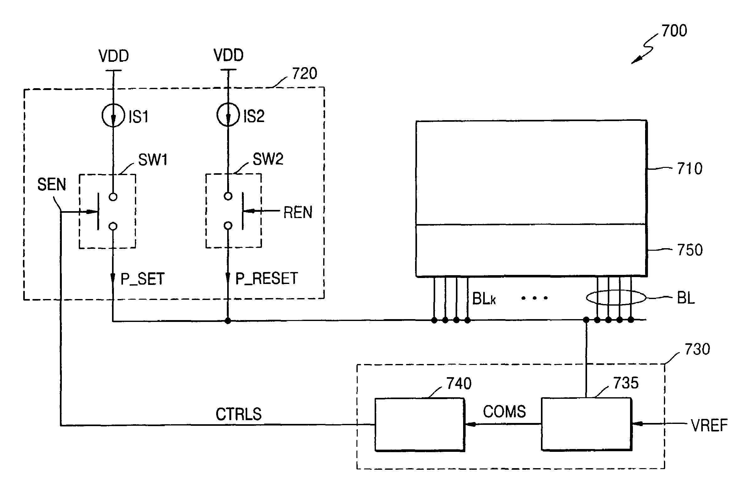
[0062]FIG. 13 is a flowchart illustrating the logical flow of a procedure for programming a PRAM cell to a set state, in accordance with the invention. The flowchart illustrates the process of automatic control of the set pulse width in accordance with this embodiment of the invention. In this procedure, the state of the PRAM cell being programmed is monitored during programming by detecting the voltage VBL on the cell bit line and comparing the bit line voltage to the reference voltage VREF. According to the procedure 600, a first pulse, e.g., the set pulse, is applied to the bit line of the cell being programmed in step 610. The voltage on the bit line VBL is monitored and compared to the reference voltage VREF, and, in step 620, while the set pulse is applied, the procedure waits for the bit line voltage VBL to be below the reference voltage VREF. When that occurs, the pulse is disconnected from the bit line in step 630.

second embodiment

[0063]FIG. 14 is a flowchart illustrating the logical flow of a procedure for programming a PRAM cell to a set state, in accordance with the invention. The flowchart illustrates the process of automatic control of the set pulse width in accordance with this embodiment of the invention. In this procedure, the state of the PRAM cell being programmed is monitored during programming by detecting the voltage VBL on the cell bit line and comparing the bit line voltage to the reference voltage VREF According to the procedure 1000, a first pulse, e.g., the set pulse, is applied to the bit line of the cell being programmed in step 1010. The resistance of the cell is monitored in step 1020, and, in step 1030, is compared to a set resistance RSET. While the set pulse is applied, the procedure waits for the resistance of the cell to be at the set resistance RSET in step 1030. When that occurs, the pulse is disconnected from the bit line in step 1040.

[0064]FIG. 15 is a flowchart illustrating the...


PUM


Abstract

A circuit and method for programming phase-change memory devices, such as chalcogenide memory (PRAM), are described. The invention is directed to an approach to programming PRAM elements from a reset state to a set state or from a set state to the set state. The invention provides a novel and nonobvious PRAM device and method in which a set pulse duration time is controlled by monitoring the state of the memory element during programming such as by comparing the voltage of a bit line with a reference voltage or comparing the cell resistance with a set state cell resistance. The duration of the set pulse is controlled in response to the detected state of the memory element. The result of the approach of the invention is the significant reduction in PRAM programming errors, such as those caused by a constant-duration set pulse, as well as reduction in programming time duration and power consumption.

Description

RELATED APPLICATION[0001]This application relies for priority on Korean patent application number 03-0035564, filed on Jun. 3, 2003, the contents of which are incorporated herein in their entirety by reference.FIELD OF THE INVENTION[0002]The present invention related to phase-change memory devices and, more particularly, to a device and method for programming a phase-change memory device using programming pulse width control.BACKGROUND OF THE INVENTION[0003]A phase change memory or phase change random access memory (PRAM) as referred to herein is also referred to as an ovonic unified memory (OUM) in the art. The OUM is based on a chalcogenide alloy, which, after being heated and cooled, adopts one of two stable but programmable phases: polycrystalline or amorphous. Resistance of the first phase, i.e., the polycrystalline phase, is low, and resistance of the second phase, i.e., the amorphous phase, is high. A logical one (1) or zero (0) depends on the phase of the programmable volume...

Claims


Application Information

Patent Timeline
Patent Type & Authority Patents(United States)
IPC IPC(8): G11C11/00G11C13/00G11C7/00G11C7/12G11C11/34G11C11/56G11C16/02G11C17/14G11C29/02H01L27/10H01L27/105H01L45/00
CPCG11C7/12G11C11/5678G11C13/0004G11C13/0026G11C13/0061G11C13/0069G11C29/02G11C29/028G11C29/50012G11C13/0064G11C2013/0092G11C2013/0066
Inventor CHO, WOO-YEONGKIM, KYUNG-HEE
Owner SAMSUNG ELECTRONICS CO LTD
Why Eureka
Try Eureka