Optical functional device and optical module
a functional device and optical module technology, applied in the field of optical functional devices and optical modules, can solve the problems difficult to align the optical coupling between elements, and difficult to provide integration, so as to achieve the effect of increasing the size of the devi
- Summary
- Abstract
- Description
- Claims
- Application Information
AI Technical Summary
Benefits of technology
Problems solved by technology
Method used
Image
Examples
first embodiment
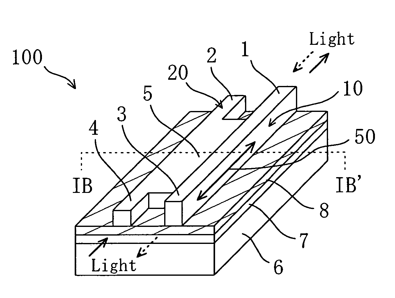
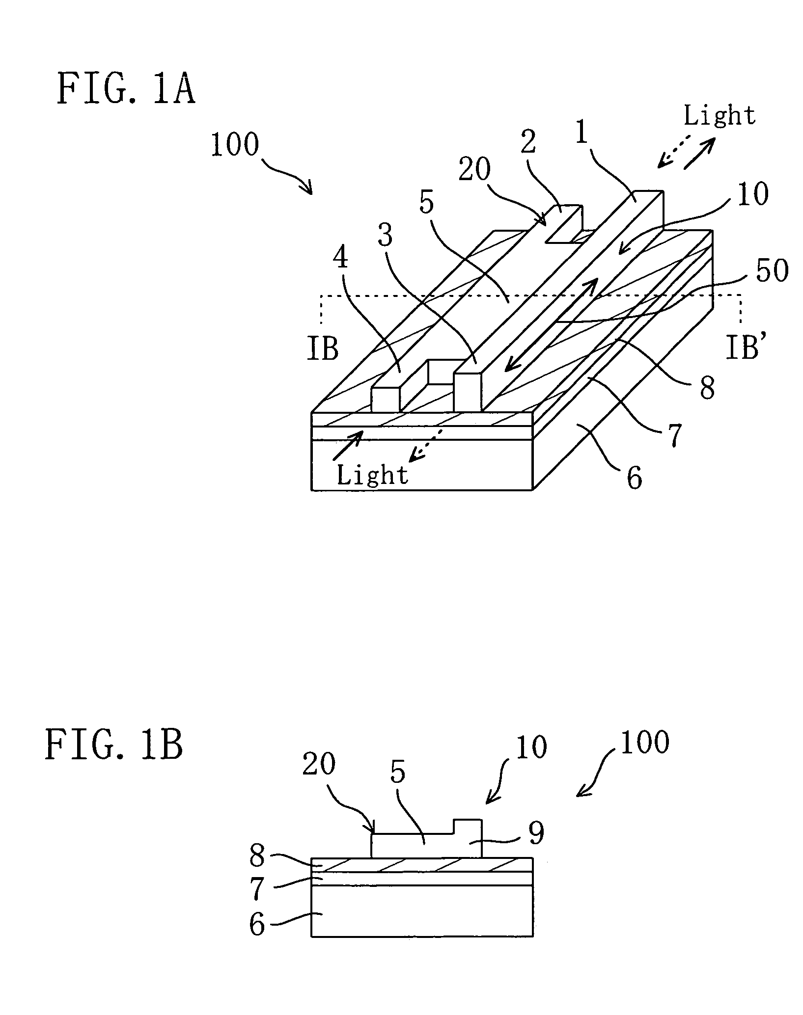
[0047]An optical functional device according to a first embodiment of the present invention will be described with reference to FIGS. 1A and 1B. FIG. 1A is an oblique view schematically illustrating the structure of an optical functional device 100 of the present embodiment, and FIG. 2B is a cross-sectional view taken along the line IB–IB′ shown in FIG. 1A.
[0048]The optical functional device 100 shown in FIGS. 1A and 1B includes: two optical waveguides (10 and 20) having mutually different equivalent refractive indices; and a connection 5 through which the two optical waveguides (10 and 20) are connected along an optical axis 50. One of the two optical waveguides will be hereinafter called a first optical waveguide 10 while the other will be hereinafter called a second optical waveguide 20, and the equivalent refractive index of the second optical waveguide 20 is lower than that of the first optical waveguide 10. It should be noted that input and output terminals of the first optica...
second embodiment
[0072]Hereinafter, an exemplary method for fabricating an optical functional device according to a second embodiment of the present invention will be described with reference to FIGS. 6 and 7. In the fabrication method according to the present embodiment, a semiconductor stacked structure is formed on a substrate, and then the semiconductor stacked structure is etched, thereby obtaining an optical functional device according to the second embodiment of the present invention.
[0073]First, as shown in FIG. 6A, an InGaAsP waveguide layer 102, an InP cladding layer 103, an InGaAsP cap layer 105, and an SiO2 layer 110 are stacked in this order over an InP substrate 101. The InGaAsP cap layer 105 includes an InP etching stop layer 106, and has a three-layer structure made up of upper and lower InGaAsP layers and the InP etching stop layer 106 sandwiched therebetween.
[0074]Next, as shown in FIG. 6B, a resist is applied to the SiO2 layer 110 and is then patterned into a predetermined shape, ...
PUM
 Abstract
Description
Claims
Application Information


