Field emission display device

a display device and field emission technology, applied in the field of display devices, can solve problems such as less than desirable emission current, and achieve the effect of increasing the emission current of current emitters

Inactive Publication Date: 2006-08-08
MICRON TECH INC
View PDF10 Cites 0 Cited by
  • Summary
  • Abstract
  • Description
  • Claims
  • Application Information

AI Technical Summary

Benefits of technology

[0010]The present invention relates to a system and method for increasing the emission current of the current emitters of a FED device by removing native oxygen from silicon deposited on the tip of the FED device through PECVD hydrogenation and subsequently incorporating nitrogen onto the surface without exposing the tip to the atmosphere.

Problems solved by technology

The result is the tip being free of approximately one third of the native oxides, which formed when the tip was exposed to atmospheric conditions and which would have otherwise remained on the tip increasing the work function and yielding a less than desirable emission current.

Method used


Image

  • Field emission display device
  • Field emission display device
  • Field emission display device

Examples


Embodiment Construction

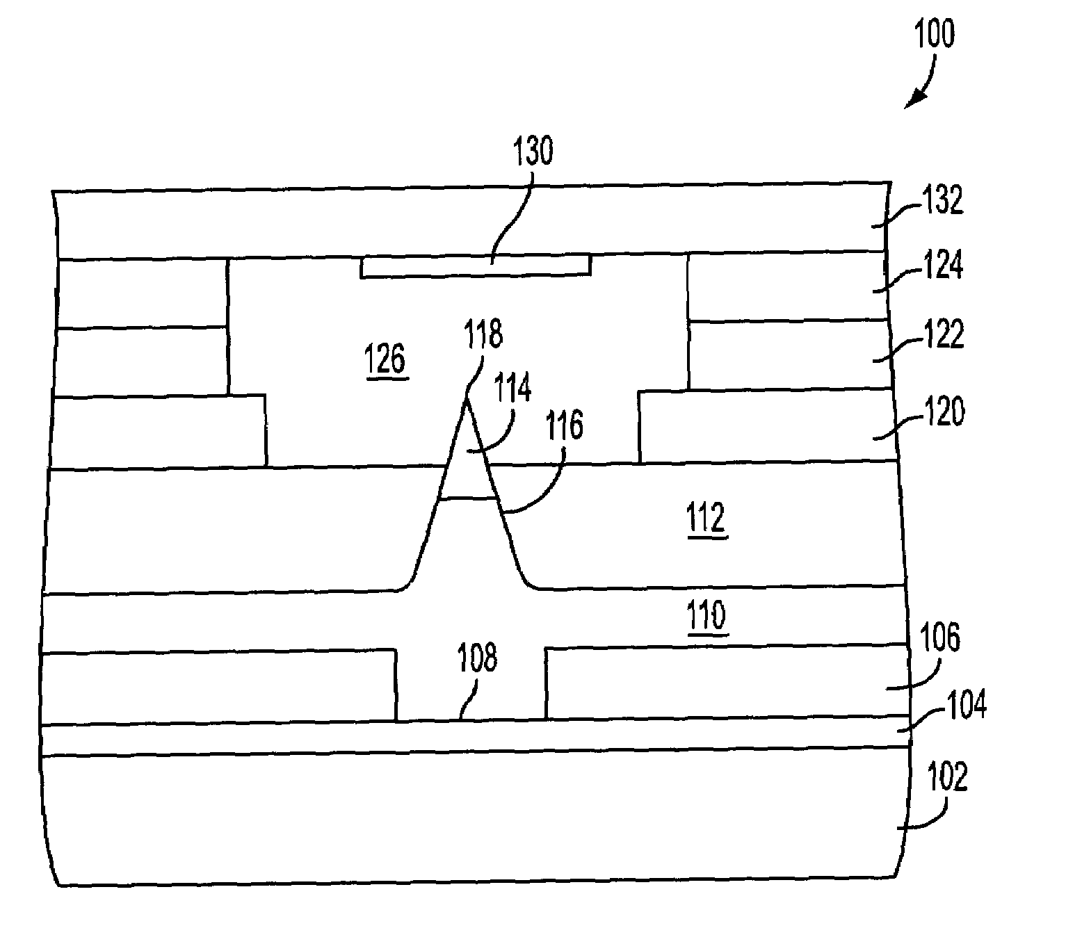
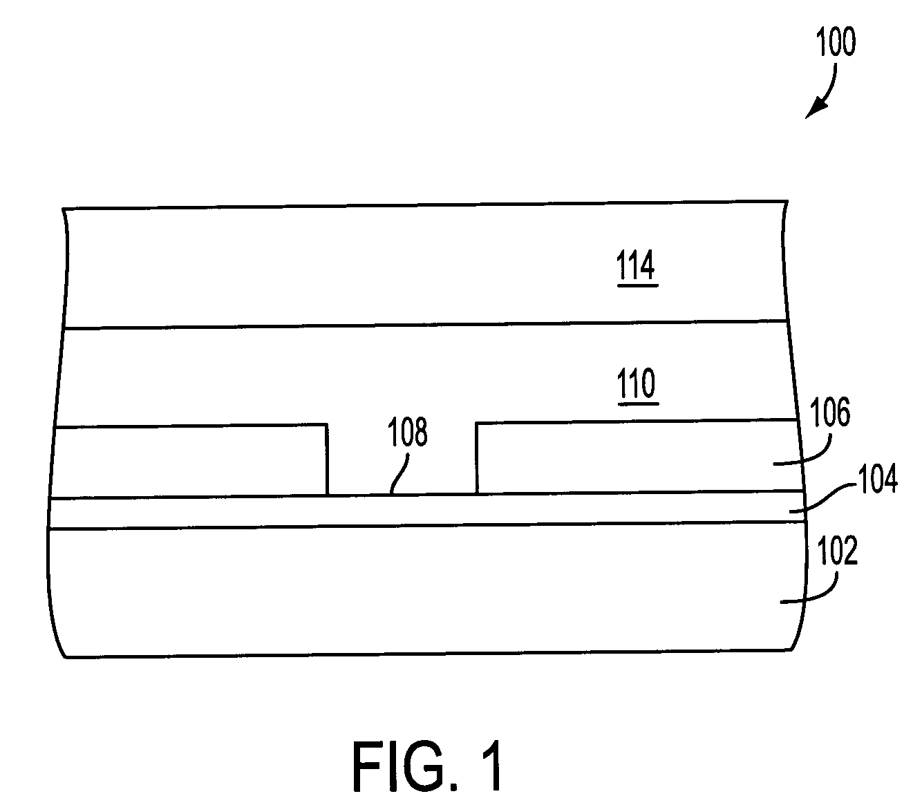
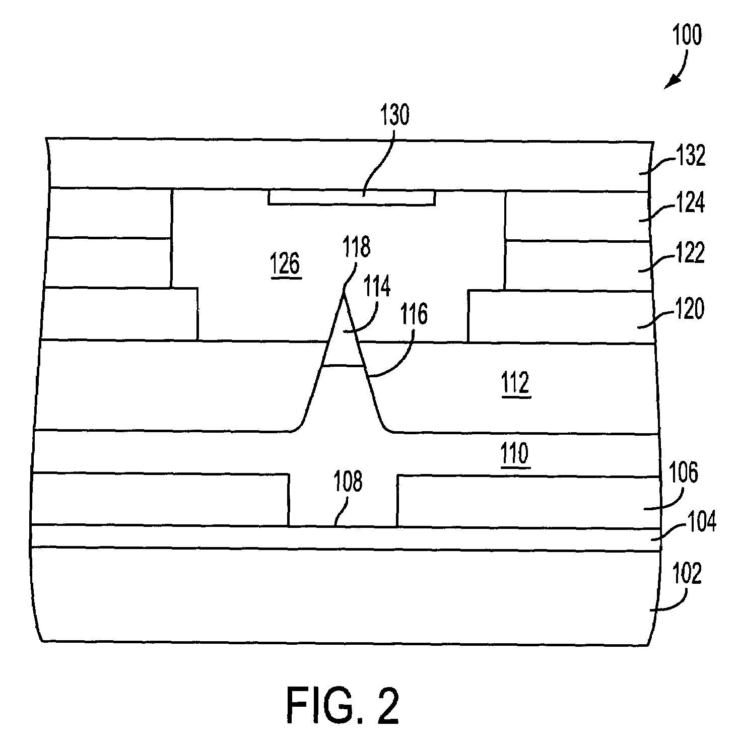
[0019]Referring now to the drawings, where like reference numerals designate like elements. FIG. 1 is a representative cross-section of a FED device 100. FED device 100 contains a substrate 102 made of glass upon which the materials making up the functional part of the FED device are deposited. The glass substrate 102 often contains impurities such as sodium, therefore, a “barrier film”104, in this instance silicon dioxide (SiO2), is deposited on top of the substrate 102 as an insulator. This barrier film 104 is deposited using PECVD processing. Next, a conductive metal layer 106 is deposited in a desired pattern on top of the barrier film 104. This conductive metal layer 106 is formed preferably of an aluminum alloy which may contain chromium. This conductive metal layer 106 is patterned to form vacant areas 108 where the conductive metal layer 106 does not cover the barrier layer 104. These vacant areas 108 will hold the base of a later formed FED tip. After conductive metal layer...


PUM

PropertyMeasurementUnit
temperatureaaaaaaaaaa
emission currentaaaaaaaaaa

Abstract

A system and method for fabricating a FED device is disclosed. The system and method provide for use of PECVD hydrogenation followed by nitrogen plasma treatment of the tip of the current emitter of the FED device. The use of this process greatly reduces the native oxides in the tip of the current emitter. Such native oxides function as undesirable insulators degrading current emission. By reducing the amount of oxides in the tip, this invention provides for an increase in the current emission of the FED device.

Description

BACKGROUND OF THE INVENTION[0001]This application is a divisional application of U.S. patent application Ser. No. 09 / 387,776, filed Sep. 1, 1999, now abandoned, the entirety of which is incorporated herein by reference.[0002]I. Field of the Invention[0003]The present invention relates generally to display devices implementing Field Emission Display (FED) technology. More specifically, the invention relates to a method for increasing the emission current of the current emitters of a Field Emission Display (FED).[0004]II. Description of the Related Art[0005]Until recently, the cathode ray tube (“CRT”) had been the primary device for displaying information. While having sufficient display characteristics with respect to color, brightness, contrast, and resolution, CRT's are relatively bulky and consume large amounts of power. In view of the advent of portable laptop computers, the demand has intensified for a display technology which is light-weight, compact, and power efficient.[0006]...

Claims


Application Information

Patent Timeline
Patent Type & Authority Patents(United States)
IPC IPC(8): H01J1/304H01J1/62H01J9/02
CPCH01J9/025
Inventor RAINA, KANWAL K.
Owner MICRON TECH INC
Why Eureka
Try Eureka