Fabrication of flat-panel display having spacer with rough face for inhibiting secondary electron escape

a technology of spacer and secondary electron escape, which is applied in the manufacture of electrode systems, tubes with screens, electrode systems, etc., can solve the problems of affecting the flow of electrons through the display, deteriorating the image produced on the viewing surface, and becoming electrically charged, so as to reduce the buildup of positive charges on the spacer, easy control of manufacturing techniques, and simple configuration

Inactive Publication Date: 2006-08-15
CANON KK +1
View PDF35 Cites 4 Cited by
  • Summary
  • Abstract
  • Description
  • Claims
  • Application Information

AI Technical Summary

Benefits of technology

[0009]The present invention furnishes a flat-panel display in which a spacer situated between a pair of plate structures has a rough face. An image is supplied by one of the plate structures in response to electrons provided from the other plate structure. Somewhat similar to what occurs in Jin et al, the roughness in the face of the present spacer prevents some secondary electrons emitted by the spacer from escaping the spacer. Accordingly, positive charge buildup on the spacer is normally reduced. The image is thereby improved.
[0012]To the extent that the spacer used in the present flat-panel display has multiple levels of spacer material, the levels typically extend vertically relative to the electron-emitting and light-emitting components rather than laterally as in Jin et al. A spacer with vertically extending spacer-material levels is generally simpler in design, and can be fabricated to high tolerances more easily, than a spacer having laterally extending spacer-material levels. When the present spacer has multiple vertically extending levels of spacer material, reliability concerns associated with the spacer design are considerably less severe than those that arise with the spacer design of Jin et al. When the spacer used in the present display has only a single level of spacer material, the display essentially avoids the reliability concerns that arise in Jin et al. The net result is a substantial improvement over Jin et al.
[0015]By inhibiting secondary electrons emitted by the present spacer from escaping the spacer, the roughness in the spacer's face also reduces spacer charging that would otherwise result from backscattered primary electrons striking the spacer. In certain embodiments of the present display, the spacer facial roughness is provided with a directional roughness characteristic that enhances the ability of the spacer's rough face to prevent secondary electrons, especially those caused by backscattered primary electrons, from escaping the spacer.
[0017]Regardless of the actual form of the roughness in the face of the spacer wall, the facial roughness can be approximated by identical cylindrical pores of pore diameter dP. The representation of the wall's facial roughness using identical pores ideally has the same total electron yield coefficient that occurs with the actual roughness in the wall's face. In this representation, the wall's facial roughness corresponds to a wall porosity of at least 10% along the wall's face and a pore height hp of at least 15% of pore height parameter hMD Parameter hMD is given by the following relationship as a function of average electric field strength EAV and pore diameter dP:hMD=√{square root over (2dP2DMD / eEAV)}where e is the electron charge, and 2DMD is the median energy of secondary electrons as they depart from (leave) the spacer wall. By using this relationship, the characteristics of the identical pores that approximate the actual roughness in the wall's face can be suitably adjusted, as electric field strength EAV changes, to reduce the number of secondary electrons that escape the spacer wall.
[0021]As another example, the main body of the spacer can be implemented with a substrate and a porous layer that overlies the substrate. The porous layer normally has an average electrical resistivity of 108–1014 ohm-cm, preferably 109–1013 ohm-cm, at 25° C. The porous layer is preferably of at least ten times greater resistance per unit length than the substrate. By implementing the main body in this way, the substrate largely determines the non-emissive electrical characteristics of the main body, while the pores largely determine the secondary electron escape characteristics of the main body. Separating these two types of spacer characteristics in this way makes it easier to design the spacer. A generally conformal coating, which typically emits a relatively low level of secondary electrons, may overlie the porous layer.
[0028]In short, the rough-faced spacer utilized in the present flat-panel display typically reduces the number of secondary electrons that escape the spacer, thereby reducing positive charge buildup on the spacer. The present spacer is of relatively simple configuration and can be manufactured according to readily controllable manufacturing techniques. The invention thus provides a large advance over the prior art.

Problems solved by technology

The presence of the spacer system can adversely affect the flow of electrons through the display.
For example, electrons coming from various sources occasionally strike the spacer system, causing it to become electrically charged.
The trajectories of electrons emitted by the electron-emitting device are thereby affected, often leading to degradation in the image produced on the viewing surface.
Although electrons are often supplied to the body from one or more other sources, the fact that the number of outgoing (secondary) electrons exceeds the number of incoming (primary) electrons commonly results in a net positive charge building up on the body.
However, the spacers in Jin et al are relatively complex and pose significant concerns in dimensional tolerance and, therefore, in reliability.
Manufacturing the spacers in Jin et al could be problemsome.

Method used


Image

  • Fabrication of flat-panel display having spacer with rough face for inhibiting secondary electron escape
  • Fabrication of flat-panel display having spacer with rough face for inhibiting secondary electron escape
  • Fabrication of flat-panel display having spacer with rough face for inhibiting secondary electron escape

Examples


Embodiment Construction

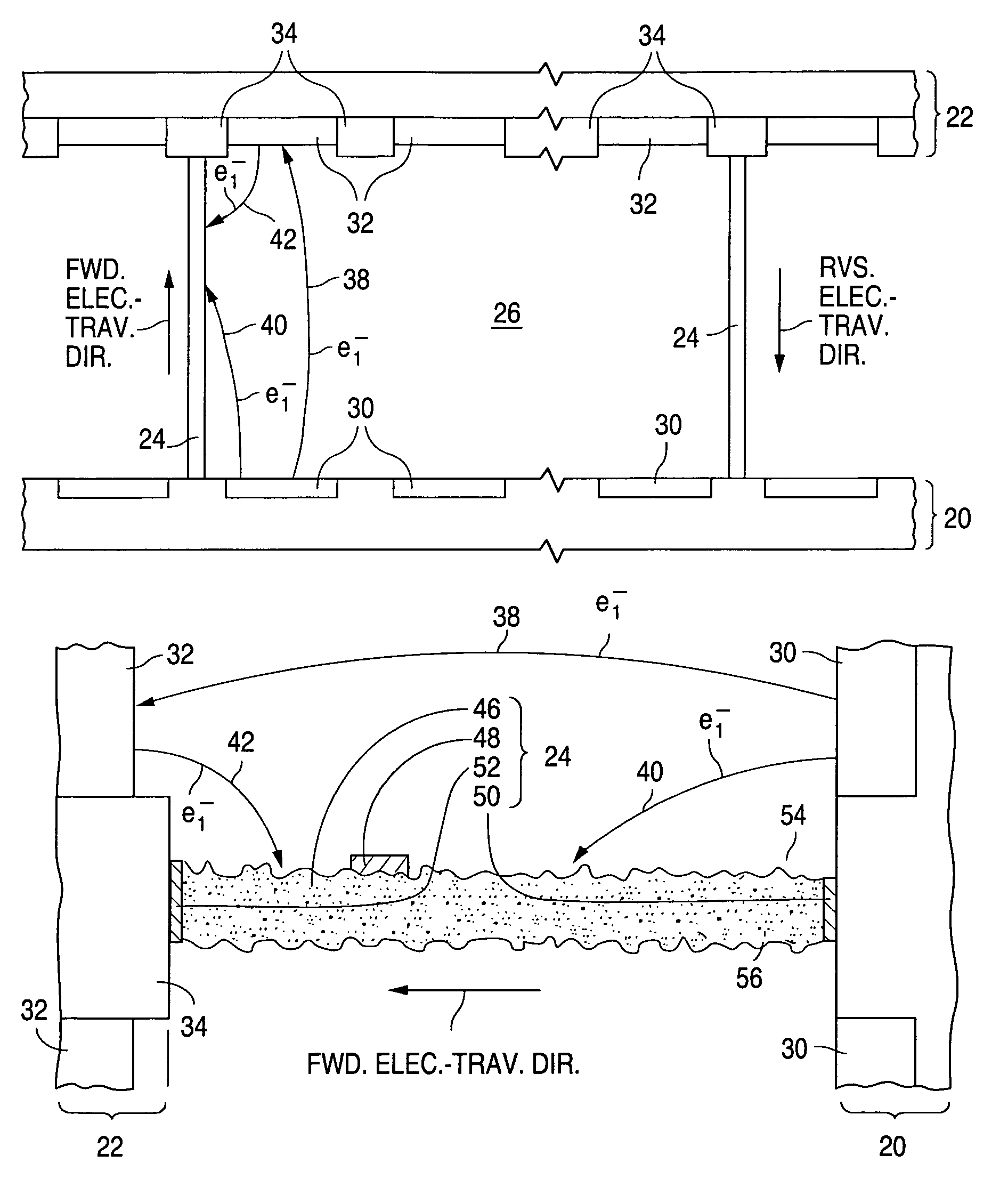
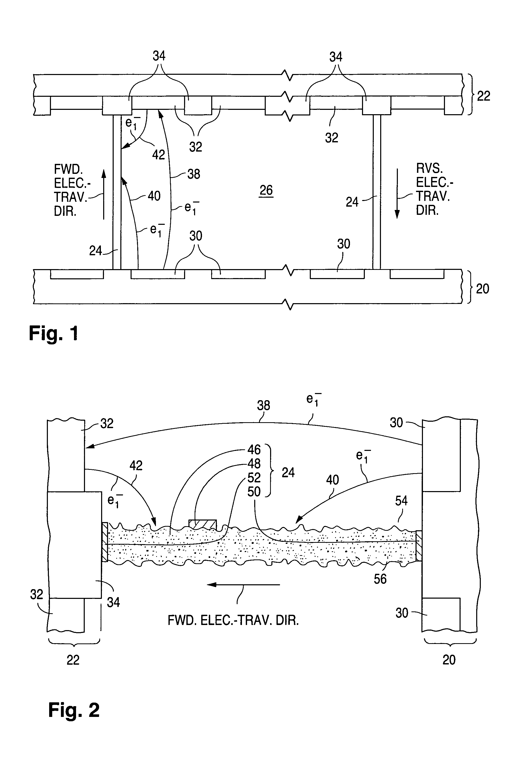
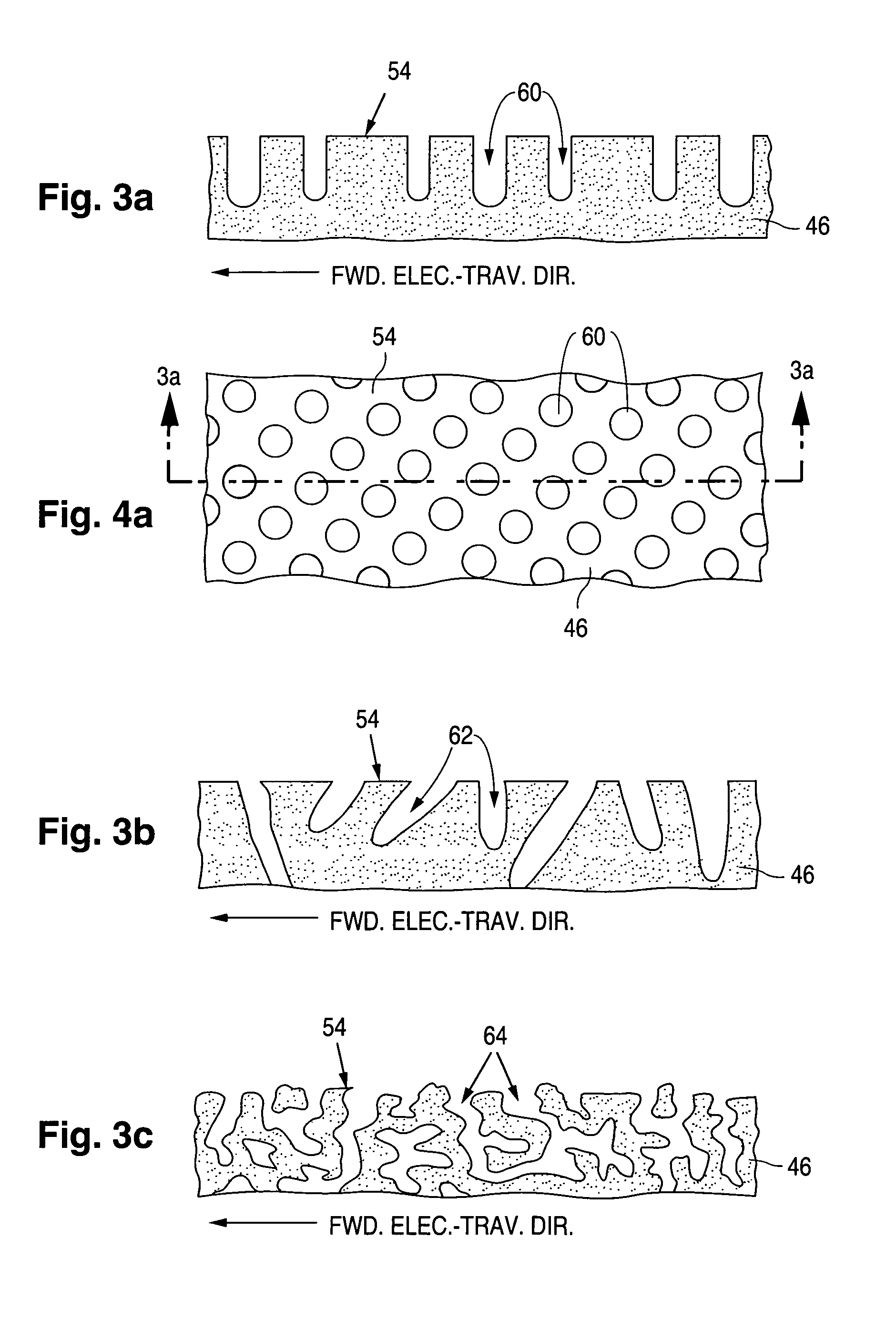
[0051]General Display Configuration An internal spacer system for a flat-panel CRT display configured and fabricated according to the invention is formed with spacers that have rough faces for reducing spacer charging during display operation. Primary electron emission in the present flat-panel CRT display typically occurs according to field-emission principles. A field-emission flat-panel CRT display (often referred to as a field-emission display) having a spacer system configured according to the invention can serve as a flat-panel television or a flat-panel video monitor for a personal computer, a lap-top computer, or a workstation.

[0052]In the following description, the term “electrically insulating” (or “dielectric”) generally applies to materials having an electrical resistivity greater than 1012 ohm-cm at 25° C. The term “electrically non-insulating” thus refers to materials having an electrical resistivity of up to 1012 ohm-cm at 25° C. Electrically non-insulating materials ...


PUM


Abstract

A flat-panel display is fabricated by a process in which a spacer (24) having a rough face (54 or 56) is positioned between a pair of plate structure (20 and 22). When electrons strike the spacer, the roughness in the spacer's face causes the number of secondary electrons that escape the spacer to be reduced, thereby alleviating positive charge buildup on the spacer. As a result, the image produced by the display is improved. The spacer facial roughness can be achieved in various ways such as providing suitable depressions (60, 62, 64, 66, 70, 74, or 80) or / and protuberances (82, 84, 88, and 92) along the spacer's face.

Description

CROSS REFERENCE TO RELATED APPLICATION[0001]This is a division of U.S. patent application Ser. No. 09 / 210,085, filed 11 Dec. 1998, now U.S. Pat. No. 6,617,772 B1.FIELD OF USE[0002]This invention relates to flat-panel displays of the cathode-ray tube (“CRT”) type, including the fabrication of flat-panel CRT displays.BACKGROUND[0003]A flat-panel CRT display basically consists of an electron-emitting component and a light-emitting component. The electron-emitting component, commonly referred to as a cathode, contains electron-emissive regions that emit electrons over a relatively wide area. The emitted electrons are suitably directed towards light-emissive elements distributed over a corresponding area in the light-emitting component. Upon being struck by the electrons, the light-emissive elements emit light that produces an image on the display's viewing surface.[0004]The electron-emitting and light-emitting components are connected together to form a sealed enclosure normally maintai...

Claims


Application Information

Patent Timeline
Patent Type & Authority Patents(United States)
IPC IPC(8): H01J9/00H01J9/24H01J29/02H01J29/86H01J31/12
CPCH01J9/242H01J29/028H01J29/864H01J31/127H01J2329/866H01J2329/8635H01J2329/864H01J2329/8645H01J2329/863
Inventor BARTON, ROGER W.NARAYANAN, KOLLENGODE S.MACKEY, BOB L.MACAULAY, JOHN M.HOPPLE, GEORGE B.SCHROPP, JR., DONALD R.NYSTROM, MICHAEL J.GOPALAKRISHNAN, SUDHAKARPEI, SHIYOUXU, XUEPING
Owner CANON KK
Why Eureka
Try Eureka