Fabrication of an EEPROM cell with SiGe source/drain regions

a technology of source/drain region and fabrication method, which is applied in the direction of basic electric elements, electrical apparatus, semiconductor devices, etc., can solve the problems of no simple and economical way to integrate these two device types into a single integrated circuit, and achieve the effect of facilitating the programming of memory transistors

a technology of source/drain region and fabrication method, which is applied in the direction of basic electric elements, electrical apparatus, semiconductor devices, etc., can solve the problems of no simple and economical way to integrate these two device types into a single integrated circuit, and achieve the effect of facilitating the programming of memory transistors

US7091075B2Inactive Publication Date: 2006-08-15ATMEL CORP

Image

  • Fabrication of an EEPROM cell with SiGe source/drain regions
  • Fabrication of an EEPROM cell with SiGe source/drain regions
  • Fabrication of an EEPROM cell with SiGe source/drain regions

Examples


Embodiment Construction

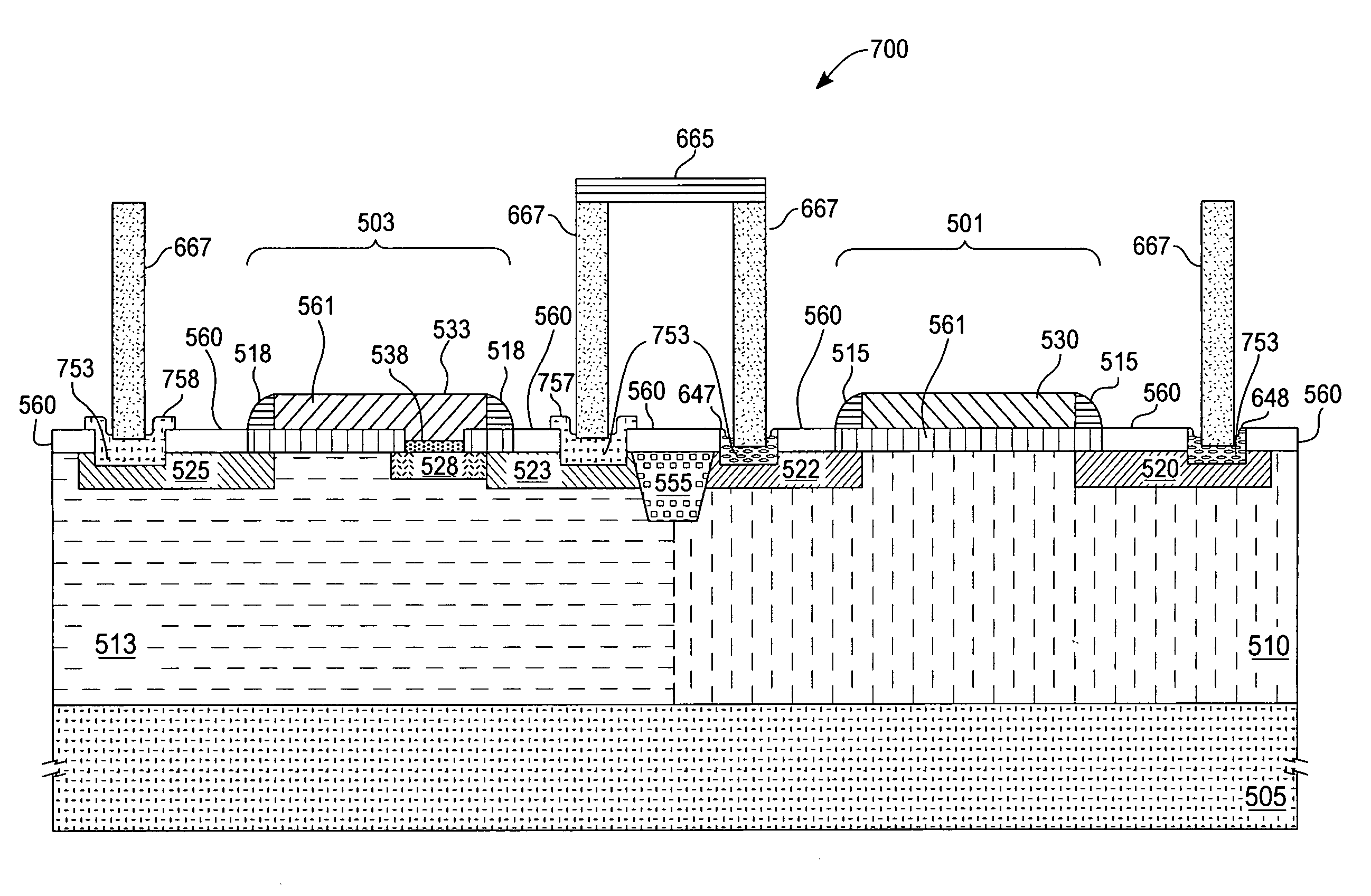
[0017]An electronic memory device of the present invention has source / drain junctions with a relatively high (e.g., about 14 volts or approximately 12–15 volts) breakdown voltage with respect to a well for a PMOS-PMOS type memory cell. The breakdown voltage of a well on a typical bipolar process is only about 10 volts. A lower well breakdown voltage is attributed to a deep (e.g., approximately 200 nm or greater (0.2 μm)) source / drain doped region. For a PMOS select device and an NMOS memory device a programming voltage of approximately 9–11 volts is produced. Using a silicon-germanium / silicon film of the present invention to fabricate source / drain regions of an MOS device results in shallow junctions and a resulting higher breakdown voltage. Therefore, the high breakdown voltage allows the present invention to be fabricated in an integrated CMOS / Bipolar (i.e., BiCMOS) line, allowing both EEPROM and BiCMOS devices to be formed in an integrated circuit.

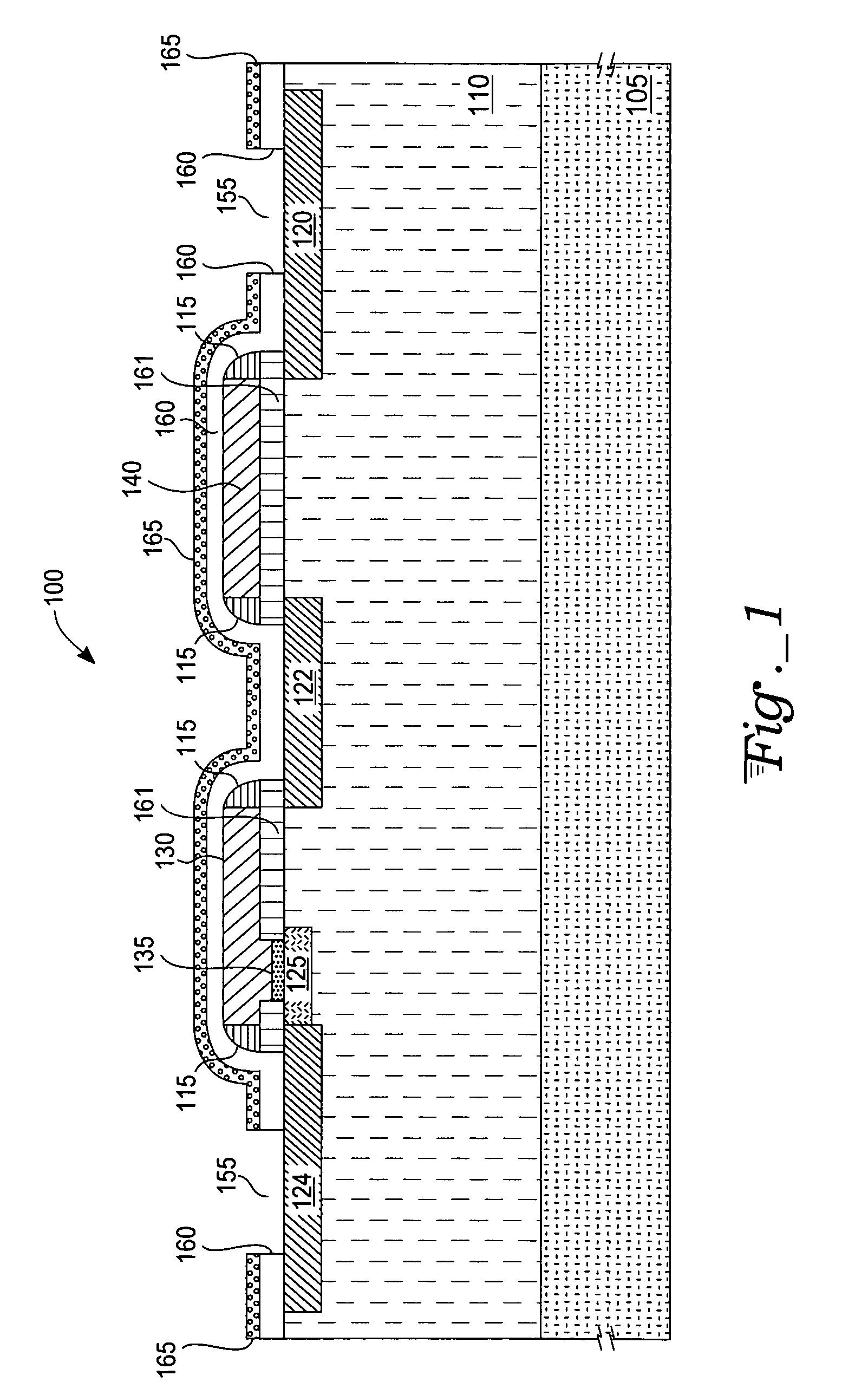
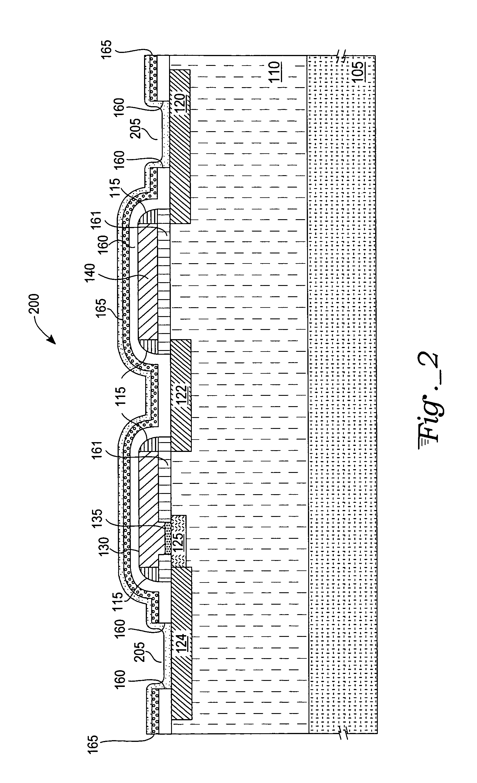
[0018]With respect to FIGS. 1–7,...


PUM


Abstract

An EEPROM memory cell uses silicon-germanium / silicon and emitter polysilicon film for fabricating shallow source / drain regions to increase a breakdown voltage with respect to a well. The source / drain regions are fabricated to be approximately 100 nm (0.1 micrometers (μm)) in depth with a breakdown voltage of approximately 14 volts or more. A typical breakdown voltage of a well in a bipolar process is approximately 10 volts. Due to the increased breakdown voltage achieved, EEPROM memory cells can be produced along with bipolar devices on a single integrated circuit chip and fabricated on a common semiconductor fabrication line.

Description

TECHNICAL FIELD[0001]The present invention relates to integrated circuit fabrication. More specifically, the present invention relates to an apparatus and method of fabrication of electrically programmable storage cells with source / drain diffusions that allow high level programming voltages.BACKGROUND ART[0002]Semiconductor memory devices are typically classified into volatile memory devices and non-volatile memory devices. Volatile memory devices are subdivided into dynamic random access memories (DRAMs) and static random access memories (SRAMs). Non-volatile memory types include mask read-only memories (MROMs), programmable read-only memories (PROMs), erasable programmable read-only memories (EPROMs), and electrically erasable programmable read-only memories (EEPROMs). Additionally, flash EEPROMs are advantageous as mass storage devices because their integration density is high compared with conventional EEPROMs.[0003]Non-volatile semiconductor memories have attained broad utiliza...

Claims


Application Information

Patent Timeline
15 Aug 2006
Publication
US7091075B2
IPC
H01L21/336
CPC
H01L27/115; H01L27/11524; H01L27/11521; H10B41/35; H10B69/00; H10B41/30
Inventors
CHAUDHRY, MUHAMMAD I.