

2V SPDT switch for high power RF wireless applications
a spdt switch and high-power rf technology, applied in the field of rf wireless applications, can solve the problems of fet switch, high insertion loss, particularly difficult, etc., and achieve the effect of minimizing distortion in a spdt switch, improving the power handling capability and harmonic performance of the switch, and minimizing distortion
- Summary
- Abstract
- Description
- Claims
- Application Information
AI Technical Summary
Benefits of technology
Problems solved by technology
Method used
Image

Examples
Embodiment Construction
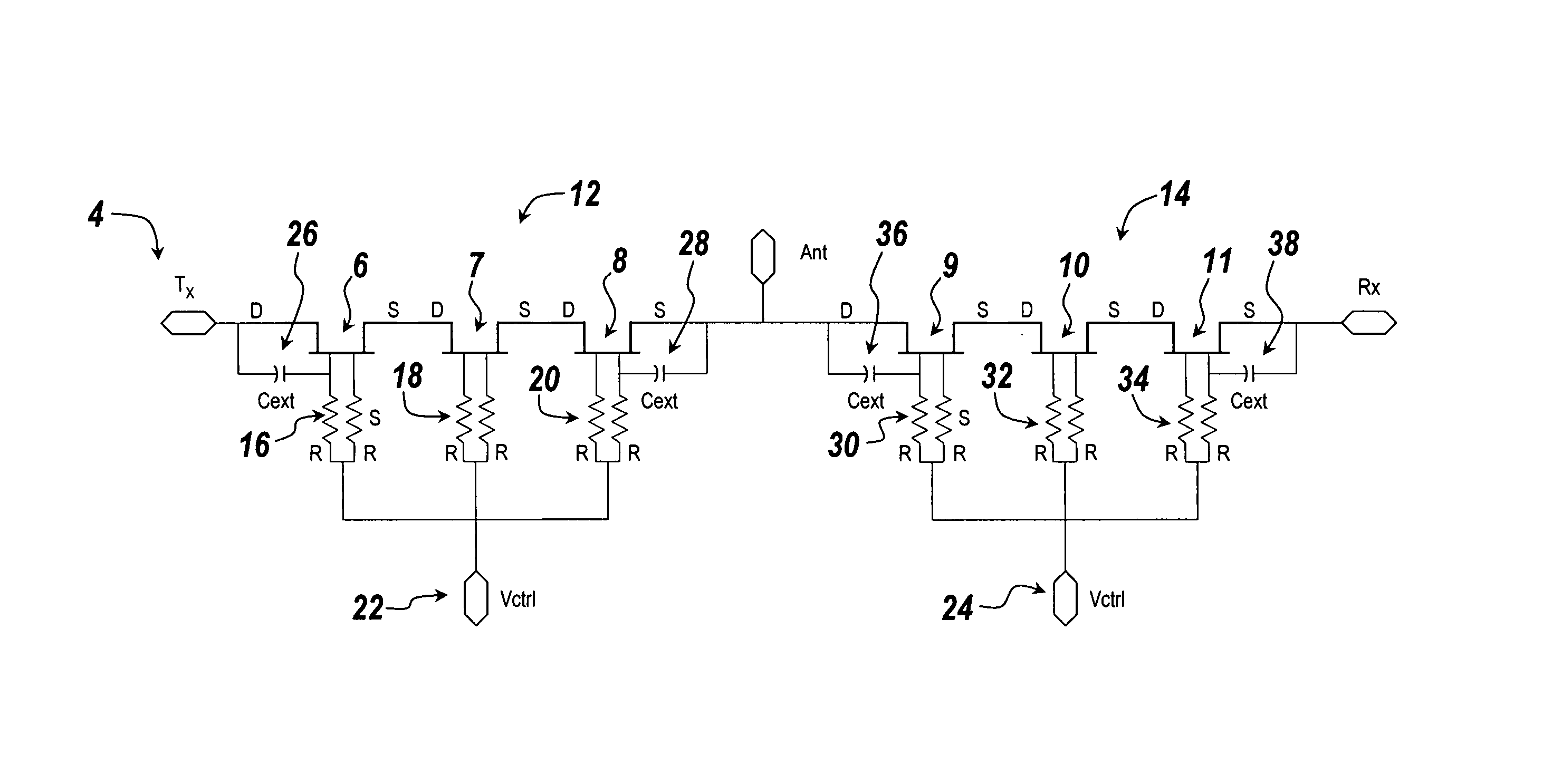
[0016]The invention is based on a new design for a transmitter-receiver (T / R) switch, which is based on field effect transistors, such as MOSFET, MESFET, or pHEMT. The invention uses 3 series dual-gate FETs, which provide reduced parasitics over a single dual-gate FET that will be described hereinbelow in FIG. 2A. The isolation of the T / R switch is increased at higher frequencies.
[0017]FIGS. 2A and 2B are a circuit diagram of a novel SPDT and a graph of the gate-to-drain voltage and gate-to-source voltage of FETs used in the novel SPDT, respectively. The SPDT 4 is divided in two sections, the transmitter section that includes all the elements on the left side of the antenna port Ant, and a receiver section that includes all the elements on the right side of the antenna port Ant. The transmitter section 12 includes FETs 6, 7, and 8, and each of these FET 6, 7, and 8 are dual gate FETs having at least two gates in this embodiment. The drain of the FET 6 is connected to the transmitter...
PUM
 Abstract
Description
Claims
Application Information