Smooth thin film layers produced by low temperature hydrogen ion cut

a thin film, low temperature technology, applied in the direction of basic electric elements, semiconductor/solid-state device manufacturing, electric devices, etc., can solve the problem of insufficient strong stiffeners

Inactive Publication Date: 2006-08-22
EPIR TECH INC
View PDF18 Cites 215 Cited by
  • Summary
  • Abstract
  • Description
  • Claims
  • Application Information

AI Technical Summary

Problems solved by technology

The stiffener formed in Bruel's work is not strong when the material is cut at temperatures of 400° C. to 600° C. Thus, a strong stiffener is not in place when the material is cut, and a rough surface results.

Method used


Image

  • Smooth thin film layers produced by low temperature hydrogen ion cut
  • Smooth thin film layers produced by low temperature hydrogen ion cut

Examples


Embodiment Construction

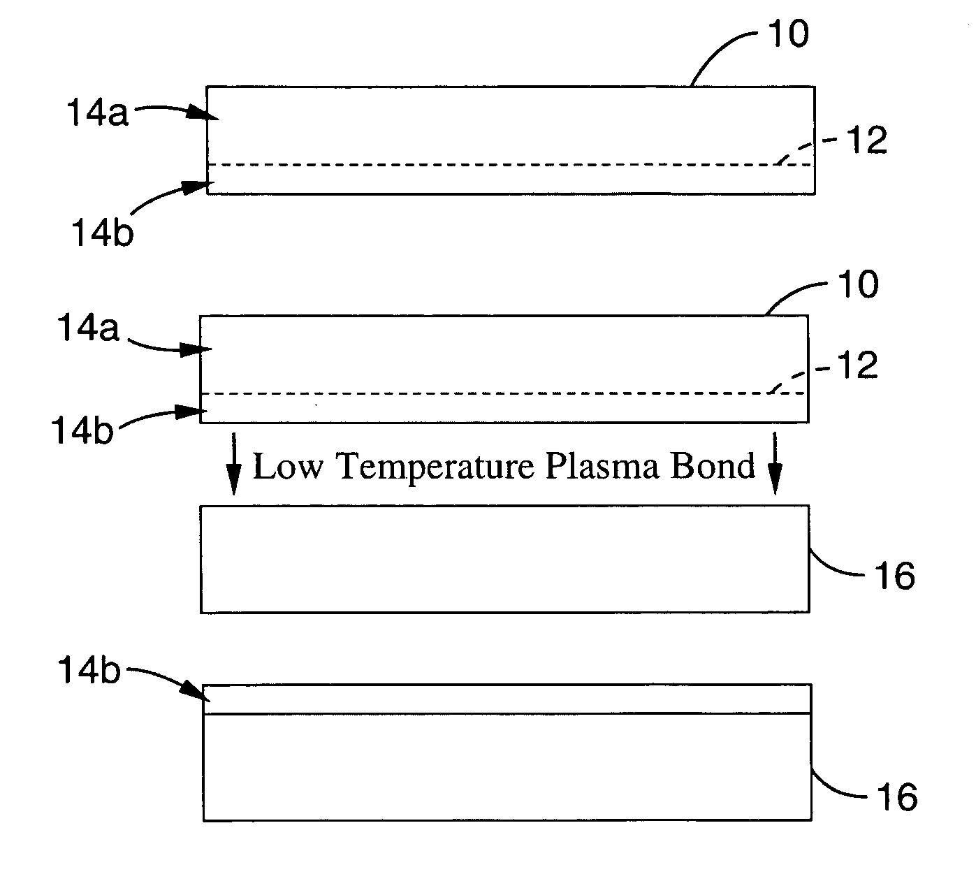
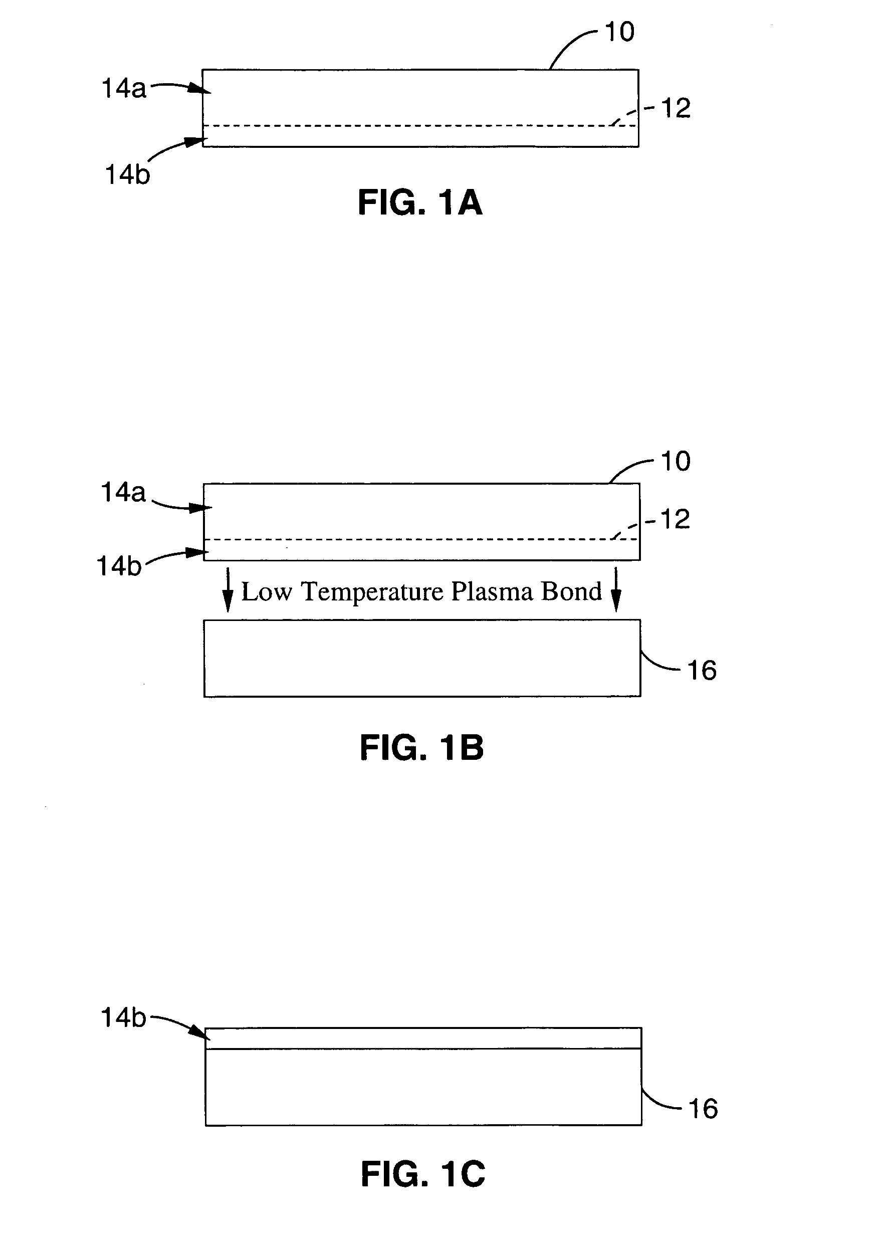
[0031]FIG. 1A through FIG. 1B show the steps for forming a smooth, thin layer of a first material that is low temperature bonded to a second material according to the present invention. Referring first to FIG. 1A, in accordance with the present invention a first material 10 is injected with ions represented by the dashed line 12. The preferred implantation technique is to ion implant hydrogen with a dose of approximately 5×10¹⁶ to approximately 1×10¹⁷ ions / cm2 at room temperature with energies in the range of approximately 22 KeV to approximately 100 KeV. The ion implantation line 12 defines a cut line between segments 14a, 14b in first material 10. Next, as shown in FIG. 1B and FIG. 1C, ion implantation is then followed by formation of a low temperature bond to a second material 16, preferably using a plasma surface treatment with oxygen as described in the literature [6–14]. Finally, as shown in FIG. 1C, first material 10 is cut along ion implantation line 12 to expunge a thin, sm...


PUM

PropertyMeasurementUnit
temperatureaaaaaaaaaa
temperaturesaaaaaaaaaa

Abstract

A method for producing wafer splitting from ion implantation into silicon after low temperature direct bonding with surface roughness that is ˜1 nm (RMS). This result is an order of magnitude smoother than the previous work (˜10 nm RMS). The key improvement in this work is the use of a low temperature bond resulting in a strong bond before the material is cut. The smooth as-split surfaces produced using a low temperature bond are very important for creation of very thin (<50 nm) silicon-on-insulator (SOI), three-dimensional bonded structures and nanostructures that are split after processing.

Description

CROSS-REFERENCE TO RELATED APPLICATIONS[0001]This application is a continuation of U.S. application Ser. No. 10 / 033,729 filed on Dec. 28, 2001 now abandoned, incorporated herein by reference, which claims priority from U.S. provisional application Ser. No. 60 / 259,061 filed on Dec. 28, 2000, incorporated herein by reference.STATEMENT REGARDING FEDERALLY SPONSORED RESEARCH OR DEVELOPMENT[0002]Not ApplicableINCORPORATION-BY-REFERENCE OF MATERIAL SUBMITTED ON A COMPACT DISC[0003]Not ApplicableBACKGROUND OF THE INVENTIONField of the Invention[0004]The present invention pertains generally to the formation of silicon-on-insulator (SOI) layers for semiconductor fabrication, and more particularly to the formation of SOI layers by using a hydrogen ion cut that follows a low temperature direct bond.INCORPORATION BY REFERENCE[0005]The following publications, some of which are referred to herein using their corresponding number inside a square bracket (e.g., [1]), are incorporated herein by refe...

Claims


Application Information

Patent Timeline
Patent Type & Authority Patents(United States)
IPC IPC(8): H01L21/00
CPCH01L21/76254H01L21/187
Inventor BOWER, ROBERT W.
Owner EPIR TECH INC
Why Eureka
Try Eureka