Semiconductor device

a technology of semiconductors and devices, applied in the direction of solid-state devices, transistors, thermoelectric devices, etc., can solve the problems of unevenness near the tft, adverse effect on display, and degradation of display quality

Inactive Publication Date: 2006-08-22
SEMICON ENERGY LAB CO LTD
View PDF17 Cites 27 Cited by
  • Summary
  • Abstract
  • Description
  • Claims
  • Application Information

AI Technical Summary

Benefits of technology

[0056]As described above, according to the present invention, the structure is used in which the TFT is covered with the light shielding film to prevent t

Problems solved by technology

When the potential of the pixel electrode is changed while the TFT is in an off state, a display quality is deteriorated.
Incidentally, in the case where the above-mentioned liquid crystal panel (in particular, a transmission type liquid crystal panel) is used for a liquid crystal projector, when light is incident into the semiconductor layer of a TFT, since a leak current due to photo-excitation (hereinafter referred to as a photo leak current) is caused, it has an adverse affect on display.
However, according to the structure disclosed in the above publication, unevenness is formed near a TFT on which various wirings are concentrated.
Thus, a possibility of reducing a yield is high because, at the time of wiring formation, a short circuit and a break of wirings are easily caused, or the wirings are easily deteriorated by the concentration of an electric field.
Thus, in the case of such a structure, there is also a possibility that a photo leak current by stray light is caused.
Further, since the concave portion is provided in the substrate, there is a possibility that the mechanical strength of the substrate is reduced.
However, in the conventional methods of forming the light shielding film between the pixel electrode and the TFT and of forming th

Method used


Image

  • Semiconductor device
  • Semiconductor device
  • Semiconductor device

Examples


embodiment mode 1

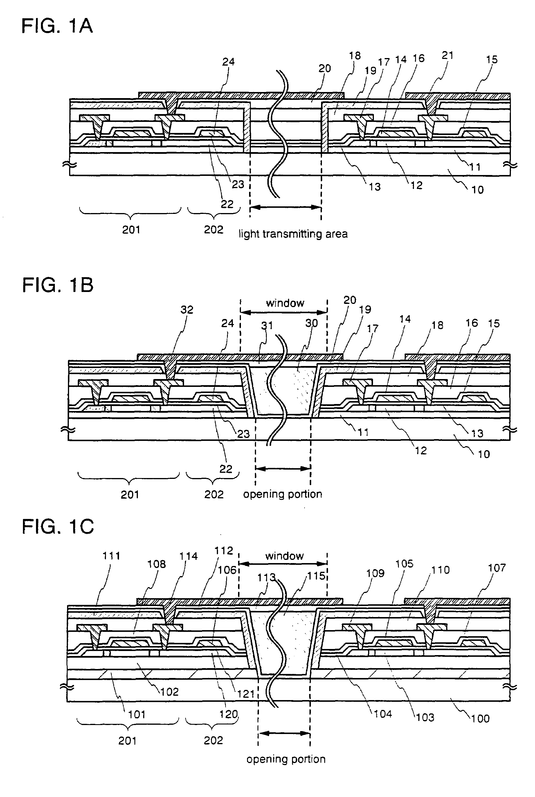
[0074]A structure of a transmission type liquid crystal display device manufactured according to the present invention will be described with reference to FIG. 1A.

[0075]A base insulating film 11 is formed on a substrate 10. A TFT composed of a semiconductor layer 12, a gate insulating film 13, and a gate electrode 14 is formed on the base insulating film 11.

[0076]A first interlayer insulating film 15 and a second interlayer insulating film 16 are formed on the gate electrode 14. The second interlayer insulating film 16 is leveled if necessary. Subsequently, a wiring 17 for electrically connecting among respective TFTs is formed to connect with the source region or the drain region of the semiconductor layer 12. A third interlayer insulating film 18 is formed to cover the wiring 17, and then a groove is formed in the boundary between the TFT and an opening portion. The groove is formed so as to reach the substrate. Next, a conductive film is continuously formed from a surface of the ...

embodiment mode 2

[0081]Another structure of a TFT of the present invention will be described with reference to FIG. 1B. Note that the same reference symbol is used in the case where the same member as in shown in FIG. 1A is indicated.

[0082]A base insulating film 11 is formed on a substrate 10. A TFT composed of a semiconductor layer 12, a gate insulating film 13, and a gate electrode 14 is formed on the base insulating film 11.

[0083]A first interlayer insulating film 15 and a second interlayer insulating film 16 are formed on the gate electrode 14. The second interlayer insulating film 16 is leveled if necessary. Subsequently, a wiring 17 for electrically connecting among respective TFTs is formed to connect with the source region or the drain region of the semiconductor layer 12. A third interlayer insulating film 18 is formed to cover the wiring 17, and then the third interlayer insulating film 18, the second interlayer insulating film 16, the first interlayer insulating film 15, the gate insulati...

embodiment mode 3

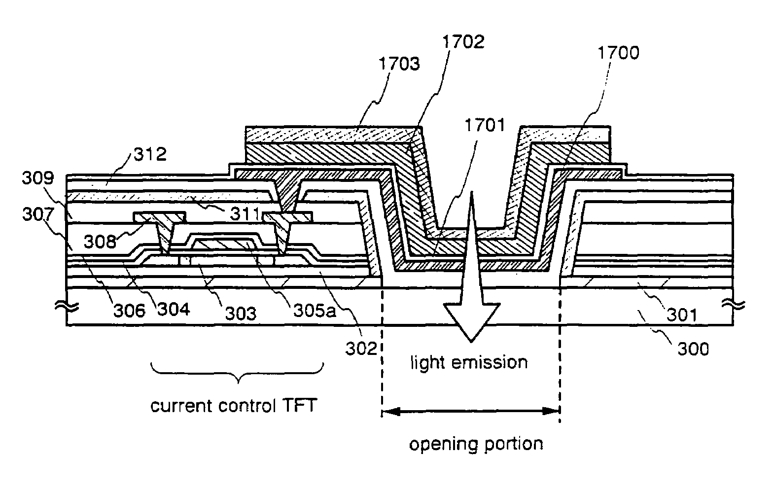
[0086]Another structure of a TFT of the present invention will be described with reference to FIG. 1C.

[0087]A lower light shielding film 101 is formed on a substrate 100. A base insulating film 102, a semiconductor layer 103, and a gate insulating film 104 are formed in order on the lower light shielding film 101. A gate electrode 105 is formed on the gate insulating film 104 and a first interlayer insulating film 107 and a second interlayer insulating film 108 are formed on the gate electrode 105. A wiring 109 connected with the source region or the drain region of the semiconductor layer 103 is formed on the second interlayer insulating film. A third interlayer insulating film 110 is formed to cover the wiring 109. An upper light shielding film 111 is provided on the third interlayer insulating film 110.

[0088]Also, a pixel electrode 114 is formed on the upper light shielding film 111 via an insulating film 112. The pixel electrode 114 is connected with a wiring connected with the ...


PUM


Abstract

Provided is a method of realizing a semiconductor device having a structure in which a sufficient light shielding property is compatible with a sufficient storage capacitance without reducing an aperture ratio. A lower light shielding film is formed on a substrate, a TFT is formed on the lower light shielding film, and an upper light shielding film is formed on the TFT via an interlayer insulating film to cover and fit the TFT. Thus, the TFT can be completely light-shielded by the lower light shielding film and the upper light shielding film and an occurrence of a photo leak current can be prevented.

Description

[0001]This application is a continuation of U.S. application Ser. No. 10 / 152,227, filed on May 21, 2002 now U.S. Pat. No. 6,734,463.BACKGROUND OF THE INVENTION[0002]1. Field of the Invention[0003]The present invention relates to a semiconductor element typically a thin film transistor (TFT), using particularly a crystalline semiconductor film as a semiconductor layer including a channel forming region, a source region, and a drain region. Also, the present invention relates to a semiconductor device using such a TFT as a driver circuit or a switching element of a pixel (particularly, a liquid crystal display device or a light emitting device) and a manufacturing technique thereof. Further, the present invention particularly relates to a semiconductor device having a structure in which a light shielding property is improved and a manufacturing technique thereof.[0004]2. Description of the Related Art[0005]In recent years, a liquid crystal projector in which characteristics such as mi...

Claims


Application Information

Patent Timeline
IPC IPC(8): H01L29/04H01L29/49H01L35/24H01L21/77H01L21/84H01L27/12H01L27/13H01L27/32H01L29/786
CPCH01L29/78633H01L51/5262H01L27/124H01L27/1255H01L27/3272H10K59/126H10K50/85
Inventor ISHIKAWA, AKIRA
Owner SEMICON ENERGY LAB CO LTD
Why Eureka
Try Eureka