Ball assignment schemes for integrated circuit packages

a technology of integrated circuits and ball assignments, applied in the field of integrated circuits, can solve the problems of increasing package size, reducing the number of signals, and not being practicable to attempt to bond such tightly packed bumps to the motherboard, so as to reduce the cost of printed circuit boards, facilitate trace routing, and increase the signal count

a technology of integrated circuits and ball assignments, applied in the field of integrated circuits, can solve the problems of increasing package size, reducing the number of signals, and not being practicable to attempt to bond such tightly packed bumps to the motherboard, so as to reduce the cost of printed circuit boards, facilitate trace routing, and increase the signal count

US7095107B2Inactive Publication Date: 2006-08-22TESSERA INC

Image

  • Ball assignment schemes for integrated circuit packages
  • Ball assignment schemes for integrated circuit packages
  • Ball assignment schemes for integrated circuit packages

Examples


Embodiment Construction

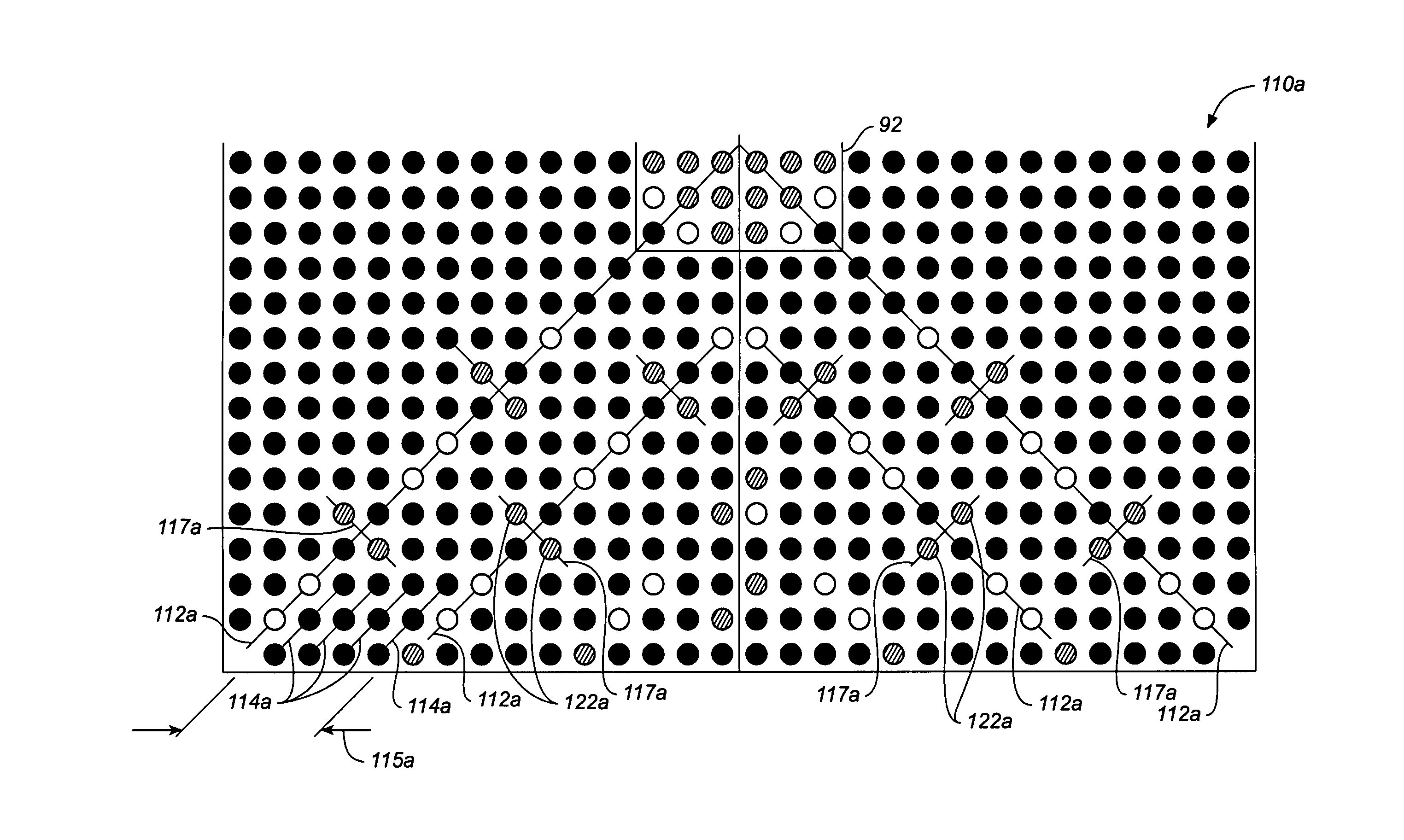
[0024]This disclosure relates to ball assignment schemes used in ball grid arrays to increase signal count and maintain quality electrical performance in various packaging technologies in integrated circuits. The disclosure, including the figures, describes the integrated circuits, ball grid arrays and ball assignment schemes, among others, with reference to several illustrative examples. Other examples are contemplated and are mentioned below or are otherwise imaginable to someone skilled in the art. The scope of the invention is not limited to the few examples, i.e., the described embodiments of the invention. Rather, the scope of the invention is defined by reference to the appended claims. Changes can be made to the examples, including alternative designs not disclosed, and still be within the scope of the claims.

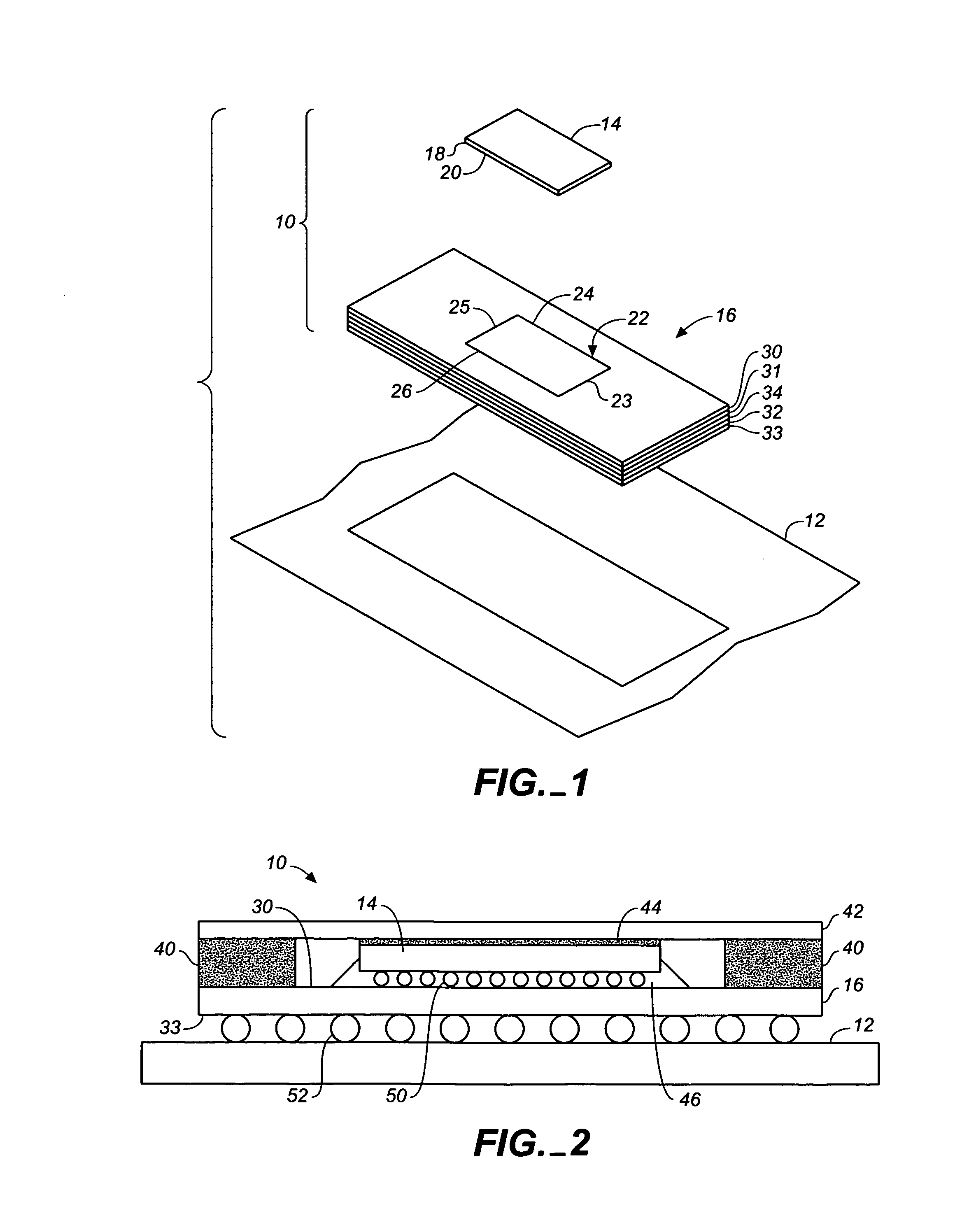
[0025]FIG. 1 is an exploded, perspective view of a flip chip 10, which can be mounted to a motherboard 12 according to one embodiment of the present disclosure. A flip ...


PUM


Abstract

The present disclosure is directed to ball assignment schemes for ball grid array packages in integrated circuits with increased signal count. The ball assignment scheme includes an array of electrical contacts. The array has a first diagonal including a pair of signal contacts adjacent to a pair of first-type voltage supply contacts. The array further includes a crossing diagonal having a pair of adjacent second-type voltage supply contacts, which crosses the first diagonal between the pair of signal contacts such that the pair of second-type voltage supply contacts oppose one another relative to the first diagonal.

Description

FIELD OF THE INVENTION[0001]The present disclosure relates to integrated circuits. More particularly, the present disclosure relates to ball assignment schemes used in ball grid array and other packages to increase signal count and maintain quality electrical performance.BACKGROUND OF THE INVENTION[0002]A ā€œflip chipā€ refers to an integrated circuit that includes at least one semiconductor die, which is bonded circuit-side down to a substrate, with direct electrical interconnection between the die and the substrate. Because the die is connected directly to the substrate, traditional bond wires are eliminated. The substrate can be a passive carrier such as a printed circuit board, or it can be another semiconductor chip. The substrate is normally bonded directly to a motherboard. Other flip chips and other integrated circuits employing a variety of more traditional packages such as lead frame packages, surface mounts, pin grid arrays and the like can also be mounted to the motherboard...

Claims


Application Information

Patent Timeline
22 Aug 2006
Publication
US7095107B2
IPC
H01L23/52; H01L23/48
CPC
H01L23/49838; H01L23/50; H01L23/528; H01L2224/73204; H01L2224/32225; H01L2224/16225; H01L2924/16195; H01L2924/15311
Inventors
RAMAKRISHNAN, ARUN; GOVIND, ANAND