

Protective layer in memory device and method therefor
a memory device and protection layer technology, applied in the field of semiconductor product manufacturing, can solve the problems of degrading the gate oxide, affecting the performance of the device, and affecting the quality of the device,
- Summary
- Abstract
- Description
- Claims
- Application Information
AI Technical Summary
Benefits of technology
Problems solved by technology
Method used
Image

Examples
Embodiment Construction
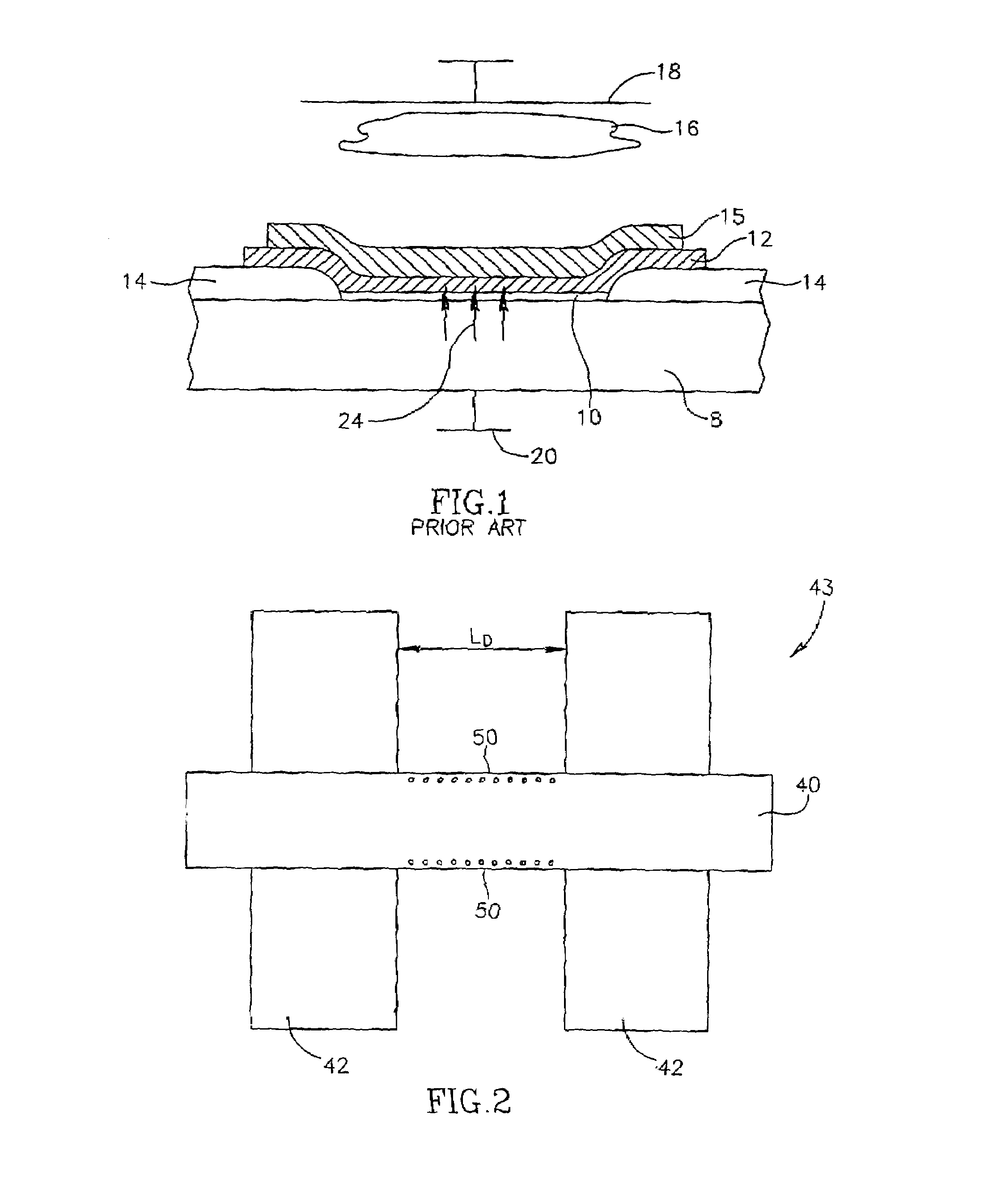
[0035]Reference is now made to FIG. 2, which illustrates a charging effect in an NROM non-volatile memory device 43, which includes one or more word lines (WL) 40 and bit lines (BL) 42. Bit lines 42 may be separated from each other by a distance LD. During etching and / or sputtering processes, portions of device 43, such as but not limited to, edges 50 of word line 40, may accumulate charge (indicated by dots along edges 50 in FIG. 2) due to the deleterious charge effect mentioned hereinabove.
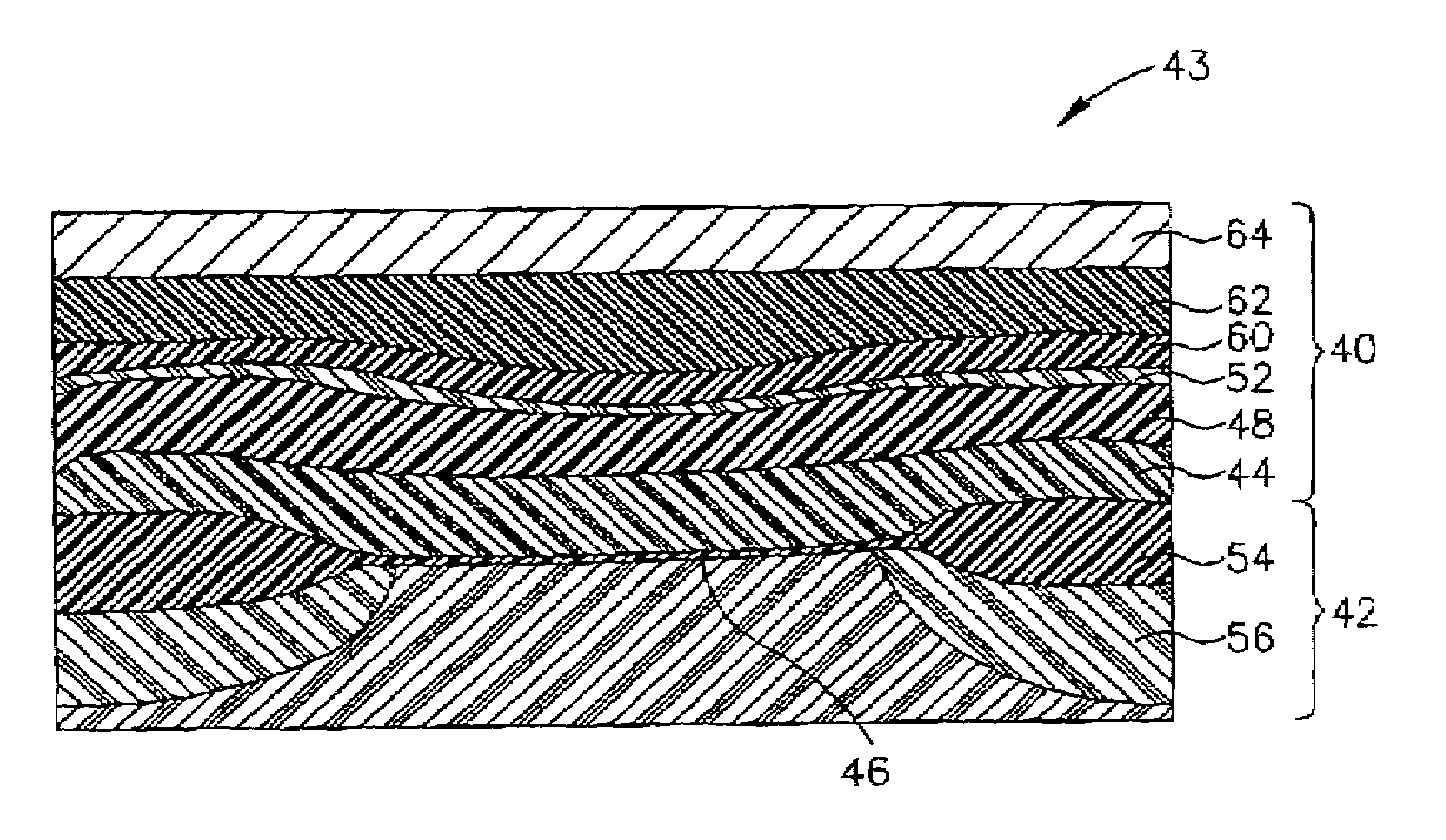
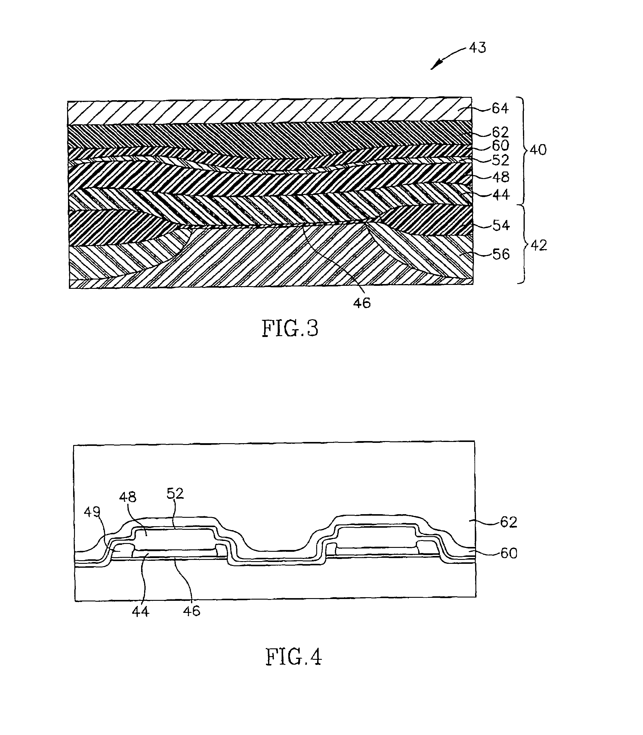
[0036]Reference is now made to FIGS. 3 and 4, which illustrate cross-sections of the NROM non-volatile memory device 43. WL 40 may comprise a polycide structure, comprising for example, a lower polysilicon layer 44 and an upper layer formed of a metal silicide film 48. Polysilicon layer 44 may comprise without limitation a polycrystalline silicon (polysilicon), which may or may not be doped with a dopant such as phosphorus, for example. Metal silicide film 48 may comprise without limitation a tu...
PUM
 Abstract
Description
Claims
Application Information