Highly integrated semiconductor device with silicide layer that secures contact margin and method of manufacturing the same

a technology of contact margin and semiconductor device, which is applied in the direction of semiconductor device, electrical apparatus, transistor, etc., can solve the problems of reducing the operating speed of the semiconductor device, reducing the resistance, and causing misalignmen

Active Publication Date: 2006-08-29
SAMSUNG ELECTRONICS CO LTD
View PDF3 Cites 21 Cited by
  • Summary
  • Abstract
  • Description
  • Claims
  • Application Information

AI Technical Summary

Problems solved by technology

Such an increase in resistance reduces the operating speed of the semiconductor device.
Because of a lack of a margin necessary for the contact hole, misalignment may occur during a photolithography process performed to form the contact hole.

Method used


Image

  • Highly integrated semiconductor device with silicide layer that secures contact margin and method of manufacturing the same
  • Highly integrated semiconductor device with silicide layer that secures contact margin and method of manufacturing the same
  • Highly integrated semiconductor device with silicide layer that secures contact margin and method of manufacturing the same

Examples


first embodiment

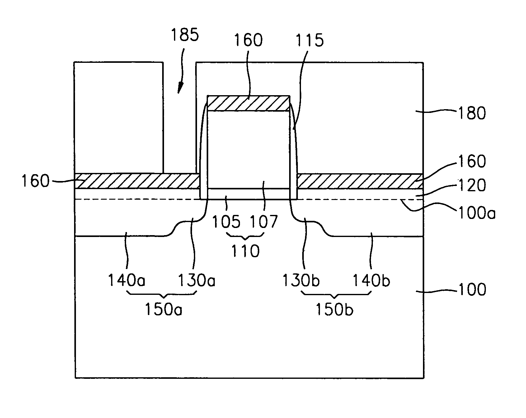
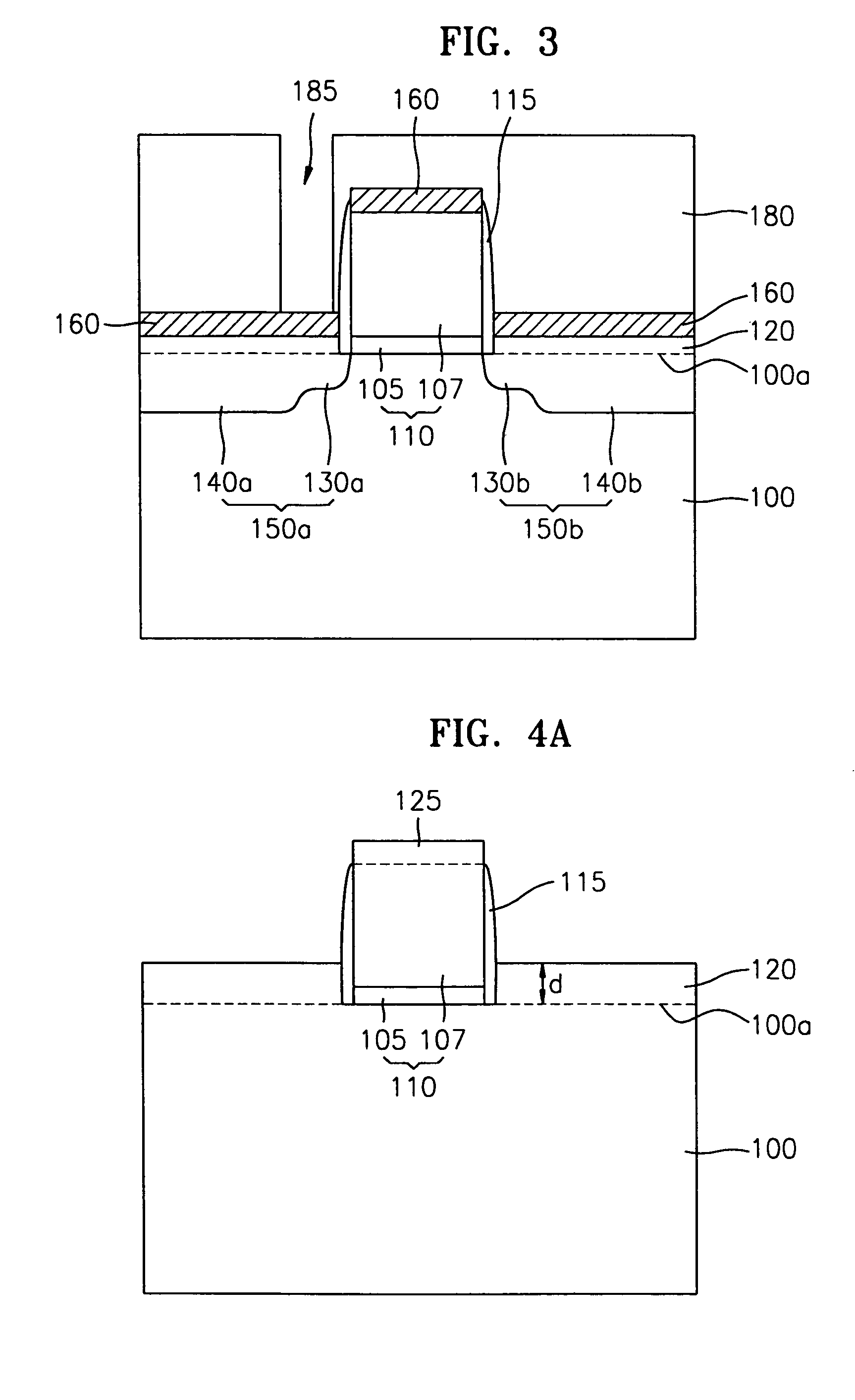
[0036]FIG. 3 is a cross-sectional view of a highly integrated semiconductor device according to the present invention, and FIGS. 4A through 4D are cross-sectional views illustrating a method of manufacturing the highly integrated semiconductor device of FIG. 3.

[0037]Referring to FIG. 3, a gate electrode 110 is formed on a semiconductor substrate 100. The semiconductor substrate 100 may be, for example, a silicon substrate or a silicon-germanium substrate. The gate electrode 110 includes a gate insulating layer 105 and a polysilicon layer 107. The gate electrode 110 is recessed a predetermined thickness into the semiconductor substrate 100. That is, the surface of the semiconductor substrate 100 on both sides of the gate electrode 110 is elevated to a predetermined thickness so as to overlap the sidewalls of the gate electrode 110. Predetermined portions of the semiconductor substrate 100 that partially overlap the sidewalls of the gate electrode 110 may be a selective epitaxial grow...

second embodiment

[0054]FIG. 6 is a cross-sectional view of a highly integrated semiconductor device according to the present invention.

[0055]In the same manner as described in the first embodiment, the silicide layer 160 is formed on the gate electrode 110, the source region 150a, and the drain region 150b. Next, a self-aligned spacer 165 is formed along the sidewalls of the offset spacer 115 that is formed along the sidewalls of the gate electrode 110. The self-aligned spacer 165 may be a silicon nitride layer, and may be thicker than the offset spacer 115.

[0056]Since a self-aligned contact (SAC) pad (not shown) can be formed on the source region 150a and the drain region 150b on the sides of the gate electrode 110 by virtue of the self-aligned spacer 165, the highly integrated semiconductor device according to the second embodiment of the present invention can be used as a transistor in a dynamic random access memory (DRAM) cell.

third embodiment

[0057]FIG. 7 is a cross-sectional view of a highly integrated semiconductor device according to the present invention.

[0058]The highly integrated semiconductor device can be formed on a silicon-on-insulator (SOI) substrate instead of the semiconductor substrate 100 made of silicon. Referring to FIG. 7, an SOI substrate 200 is prepared. The SOI substrate 200 includes a base substrate 210, a silicon oxide film-buried layer 220, and a silicon layer. 230. The SOI substrate 200 can be formed by bonding two wafers or implanting oxygen into a wafer using ion implantation.

[0059]Next, the gate electrode 110 and the source and drain regions 150a and 150b are sequentially formed in the SOI substrate 200 in the same manner as described in the first embodiment of the present invention. Since the silicon layer 230 of the SOI substrate 200 has the same properties as the semiconductor substrate 100 of the first embodiment of the present invention, the highly integrated semiconductor device can be m...


PUM


Abstract

Provided are a highly integrated semiconductor device with a silicide layer, which can secure a contact margin, and a method of manufacturing the highly integrated semiconductor device. The highly integrated semiconductor device includes a gate electrode formed on a semiconductor substrate. A source region and a drain region are formed in predetermined upper portions of the semiconductor substrate on two sides of the gate electrode such that each of the source region and the drain region includes a lightly doped drain (LDD) region and a heavily doped region. A suicide layer is formed on the gate electrode, the source region, and the drain region. The silicide layer has a sufficient thickness to function as an ohmic contact and is formed on the LDD region and the heavily doped region of each of the source region and the drain region.

Description

BACKGROUND OF THE INVENTION[0001]This application claims the priority of Korean Patent Application No. 2003-58287, filed on Aug. 22, 2003, in the Korean Intellectual Property Office, the disclosure of which is incorporated herein in its entirety by reference.[0002]1. Field of the Invention[0003]The present invention relates to a highly integrated semiconductor device and a method of manufacturing the highly integrated semiconductor device, and more particularly, to a highly integrated semiconductor device with a silicide layer that can secure a contact margin, and a method of manufacturing the highly integrated semiconductor device.[0004]2. Description of the Related Art[0005]As the degree of integration of a semiconductor device increases, the area and line width of the semiconductor device decreases, resulting in an increase of an interconnection resistance and a contact resistance of the semiconductor device.[0006]Such an increase in resistance reduces the operating speed of the ...

Claims


Application Information

Patent Timeline
Patent Type & Authority Patents(United States)
IPC IPC(8): H01L29/76H01L29/94H01L31/62H01L31/113H01L31/119H01L21/28H01L21/24H01L21/336H01L29/417H01L29/78H01L29/786H01L31/062
CPCH01L29/665H01L29/6653H01L29/6656H01L29/6659H01L29/66628H01L29/7833H01L21/24H01L29/7835
Inventor OH, MYOUNG-HWANKO, YOUNG-GUN
Owner SAMSUNG ELECTRONICS CO LTD
Why Eureka
Try Eureka