Alignment marks with salicided spacers between bitlines for alignment signal improvement

a technology of alignment signal and spacer, which is applied in the field of photolithography, can solve the problems of reducing the resolution in the area, reducing the cost and processing time, and not being common in modern semiconductor fabrication of contact printing, so as to achieve enhanced optical contrast

Active Publication Date: 2006-08-29
INFINEON TECH LLC
View PDF4 Cites 3 Cited by
  • Summary
  • Abstract
  • Description
  • Claims
  • Application Information

AI Technical Summary

Benefits of technology

[0024]The present invention pertains to utilizing a salicide in establishing alignment marks. A metal layer is formed over exposed portions of a silicon substrate as well as oxide areas formed over bitlines buried within the substrate. The metal layer is treated to react with the exposed portions of the silicon substrate to form salicided areas. The metal layer does not, however, react with the oxide areas. As such, salicided areas are formed adjacent to the oxide areas to reveal a stark optical contrast when light is shined there-upon. In this manner, the alignment marks can be very easily “seen”. The enhanced optical contrast allows the marks to continue to be seen as scaling continues.

Problems solved by technology

To prevent this problem, the masks 706 must be inspected and cleaned regularly which can be disadvantageous, at least, in terms of cost and processing time.
This particulate contamination can result in reduced resolution in the area local to the foreign particle.
Consequently, contact printing is not common in modern semiconductor fabrication.
Unfortunately, as the gap 822 increases, the resolution of the proximity printing system 800 rapidly deteriorates.
Since many integrated circuits today require features of 0.25 micrometers or less, proximity printing 800 is not considered adequate for many modern semiconductor fabrication processes.
Consequently, the size of the wafer is no longer a consideration for the system optics.
Although step and scan systems constitute an improvement in pattern transfer quality, the scanning process can contribute to pattern transfer errors in one or more directions (e.g., the X-direction)) if the subsystem 1106 positioning is not proper for each scan.
Furthermore, instability in such scanning systems can lead to errors in pattern transfer.
As will become apparent in the discussion that follows, however, conventional alignment mark structures suffer from some disadvantages which prevent alignment accuracy from being maximized.

Method used


Image

  • Alignment marks with salicided spacers between bitlines for alignment signal improvement
  • Alignment marks with salicided spacers between bitlines for alignment signal improvement
  • Alignment marks with salicided spacers between bitlines for alignment signal improvement

Examples


Embodiment Construction

[0039]One or more aspects of the present invention are described with reference to the drawings, wherein like reference numerals are generally utilized to refer to like elements throughout, and wherein the various structures are not necessarily drawn to scale. In the following description, for purposes of explanation, numerous specific details are set forth in order to provide a thorough understanding of one or more aspects of the present invention. It may be evident, however, that one or more aspects of the present invention may be practiced with a lesser degree of these specific details. In other instances, well-known structures and devices are shown in block diagram form in order to facilitate describing one or more aspects of the present invention.

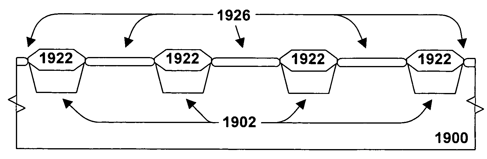
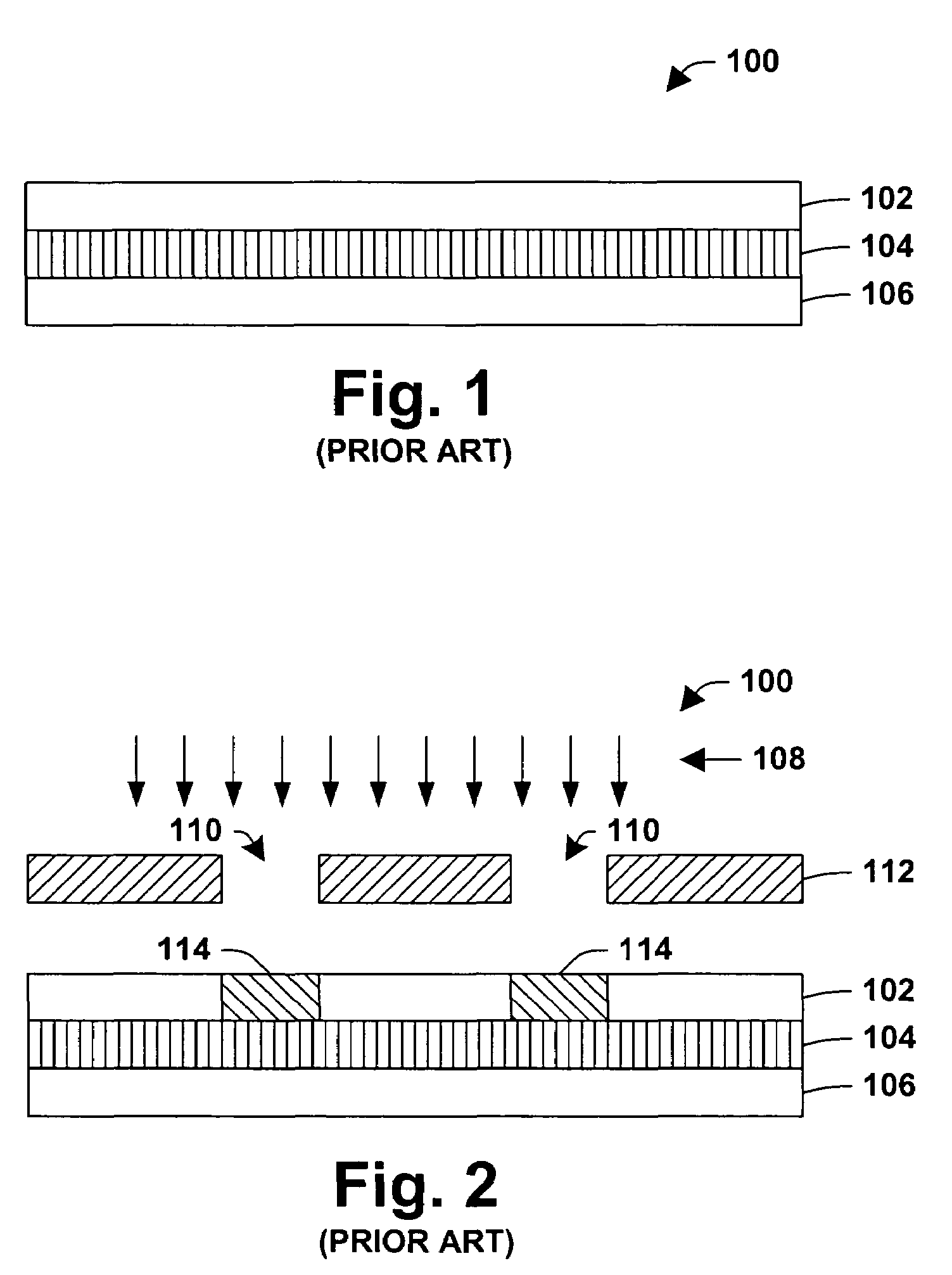
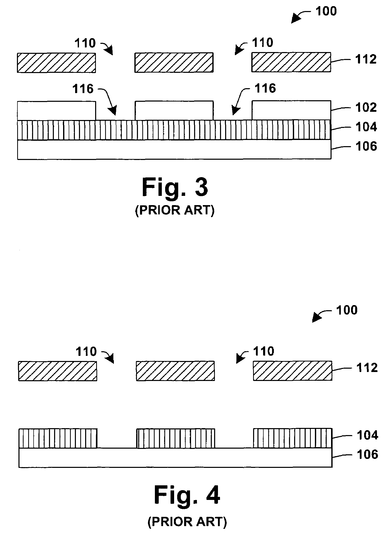
[0040]The present invention pertains to utilizing a salicide to improve optical contrast about an oxide of an alignment mark. More particularly, portions of a substrate adjacent to oxide areas formed over bitlines buried within the sub...


PUM

PropertyMeasurementUnit
widthsaaaaaaaaaa
areasaaaaaaaaaa
charge-trapping dielectricaaaaaaaaaa

Abstract

The present invention pertains to utilizing a salicide in establishing alignment marks in semiconductor fabrication. A metal layer is formed over exposed portions of a silicon substrate as well as oxide areas formed over bitlines buried within the substrate. The metal layer is treated to react with the exposed portions of the silicon substrate to form salicided areas. The metal layer does not, however, react with the oxide areas. As such, salicided areas are formed adjacent to the oxide areas to provide an enhanced optical contrast when light is shined there-upon. In this manner, the alignment marks can be more readily “seen”. The enhanced optical contrast thus allows the marks to continue to be seen as scaling occurs.

Description

FIELD OF INVENTION[0001]The present invention relates generally to photolithography, and more particularly to utilizing salicides in a photolithographic process to establish alignment marks and facilitate improved alignment and registration in a semiconductor fabrication process.BACKGROUND OF THE INVENTION[0002]In the semiconductor industry, there is a continuing trend toward higher device densities. To achieve these higher densities there has been, and continues to be, efforts toward scaling down and packing more devices on semiconductor wafers. In order to accomplish higher device packing densities, the respective sizes of features making up these devices have to be reduced. This may include reducing the width and spacing of interconnecting lines and the surface geometry such as the corners and edges of various features.[0003]The requirement of small features with close spacing between adjacent features requires high resolution photolithographic processes. In general, lithography ...

Claims


Application Information

Patent Timeline
Patent Type & Authority Patents(United States)
IPC IPC(8): H01L23/544H01L21/76
CPCG03F7/70633G03F9/7076G03F9/708G03F9/7084H01L27/115H01L27/11568H01L23/544H01L2924/3011H01L2223/54453H01L2924/0002H10B43/30H10B69/00H01L2924/00
Inventor LINGUNIS, EMMANUIL H.YANG, JEAN YEE-MEISHIRAIWA, HIDEHIKO
Owner INFINEON TECH LLC
Why Eureka
Try Eureka