Method for optimizing photoetching registration accuracy of emitting electrode of silicon germanium HBT (heterojunction bipolar transistor)

An alignment accuracy and emitter technology, applied in the field of photolithography, can solve the problems of poor stability, unstable mass production, and difficulty in improving photolithography alignment accuracy, so as to enhance optical contrast and avoid optical alignment accuracy. Measurement Error and Effects of Instability

Active Publication Date: 2015-02-04
SHANGHAI HUAHONG GRACE SEMICON MFG CORP
View PDF6 Cites 1 Cited by
  • Summary
  • Abstract
  • Description
  • Claims
  • Application Information

AI Technical Summary

Problems solved by technology

However, in high-frequency devices, in order to reduce parasitic capacitance, the emitter opening film layer is usually very thin. At this time, sufficient optical contrast cannot be formed, resulting in weak lithography alignment signals, making lithography alignment accuracy difficult. Improvement, while poor stability, unstable mass production

Method used


Image

  • Method for optimizing photoetching registration accuracy of emitting electrode of silicon germanium HBT (heterojunction bipolar transistor)
  • Method for optimizing photoetching registration accuracy of emitting electrode of silicon germanium HBT (heterojunction bipolar transistor)
  • Method for optimizing photoetching registration accuracy of emitting electrode of silicon germanium HBT (heterojunction bipolar transistor)

Examples


Embodiment Construction

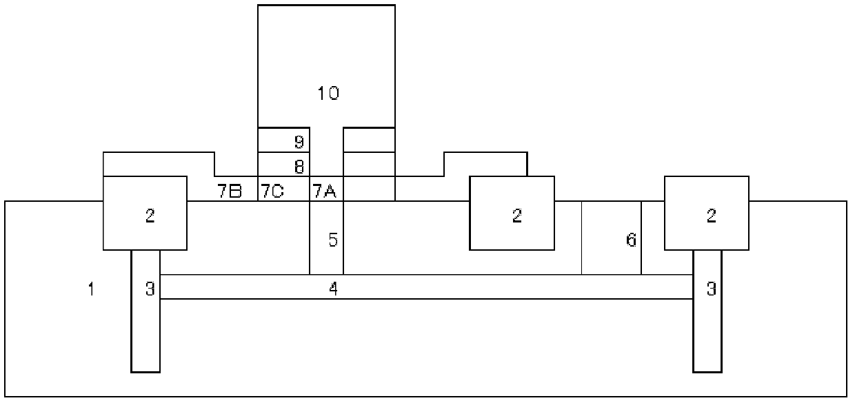
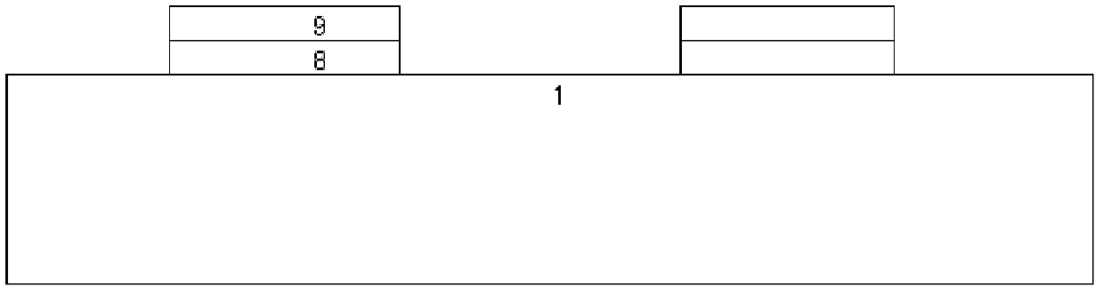
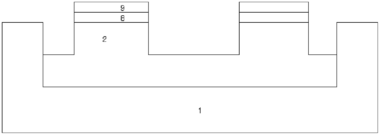
[0034] The method for optimizing the photolithographic alignment accuracy of the silicon germanium HBT emitter according to the present invention, the preparation process of the photolithographic alignment mark and the OVLmark is as follows:

[0035] 1. Photolithography etches the silicon substrate to produce grooves with a depth of preferably

[0036] 2. Fill the trench with SiO 2 and planarize to remove the SiO in the non-trench area 2 ;

[0037] 3. Deposit the buffer layer SC between BP and the substrate (SiO2+SiN or SiO2+Poly, the thickness is SiO2 Upper material ), etch the SC layer, open the device area, and produce two groups of patterns of etching and non-etching in the photolithographic pattern area.

[0038] 4. Deposit BP film (Si / Ge) and etch it, and dry etch the barrier layer SiO 2 , until SiO 2 stop, residual SiO 2 for

[0039] 5. Deposit the emitter opening film on the silicon substrate (active area), and the lower layer is SiO 2 , usually pref...


PUM


Abstract

The invention discloses a method for optimizing the photoetching registration accuracy of an emitting electrode of silicon germanium HBT ((heterojunction bipolar transistor). A photoetching registration mark and an overlaying accuracy measuring mark OVL mark of an opening layer of the emitting electrode are both placed in a field area. The process procedure includes that an active area photoetches and produces a substrate area of the registration mark and the overlaying accuracy measuring mark OVL mark of an opening of the emitting electrode; a substrate consisting of a SiO2 material of the registration mark and the overlaying accuracy measuring mark OVL mark of the opening of the emitting electrode is formed by depositing of SiO2 deposits and the CMP(chemical mechanical planarization); a base area BP is etched in front of the opening of the emitting electrode, and an opening film layer of the emitting electrode deposits after the base area BP etching; and wet etching is added after the photoetching of the opening of the emitting electrode. By the aid of the method, optical contract can be greatly strengthened, and errors and instability of optical alignment accuracy measurement caused by insufficient signal intensity are avoided.

Description

technical field [0001] The invention relates to a manufacturing method of a germanium-silicon Si / Ge heterojunction bipolar transistor HBT in the field of electronic chip manufacturing, in particular to a photolithography method. Background technique [0002] Si is currently one of the most important materials for mass-produced semiconductor devices. It is easy to prepare raw materials, rich in nature, and has basic characteristics such as semiconductor characteristics, so it is used to prepare semiconductor devices. [0003] However, for high-frequency and high-speed applications, the bandgap of Si is wide, and the mobility of carriers is restricted. Therefore, people usually introduce some other elements to form Si alloys to reduce the bandgap and increase the mobility of carriers. Among them Ge is one of the most important and main materials. Ge has a crystal structure similar to Si, and the alloying process with Si is easy to implement and highly compatible. At the same ...

Claims


Application Information

Patent Timeline
Patent Type & Authority Patents(China)
IPC IPC(8): H01L21/331H01L23/544G03F9/00
Inventor 王雷
Owner SHANGHAI HUAHONG GRACE SEMICON MFG CORP
Why Eureka
Try Eureka