Integrated circuit with dual eye openers

a technology of integrated circuits and eye openers, applied in the field of data integrity assurance, can solve the problems of increasing jitter, increasing jitter beyond an acceptable threshold or budget, and increasing jitter at higher frequencies, so as to reduce jitter

Active Publication Date: 2006-08-29
II VI DELAWARE INC
View PDF14 Cites 98 Cited by
  • Summary
  • Abstract
  • Description
  • Claims
  • Application Information

AI Technical Summary

Benefits of technology

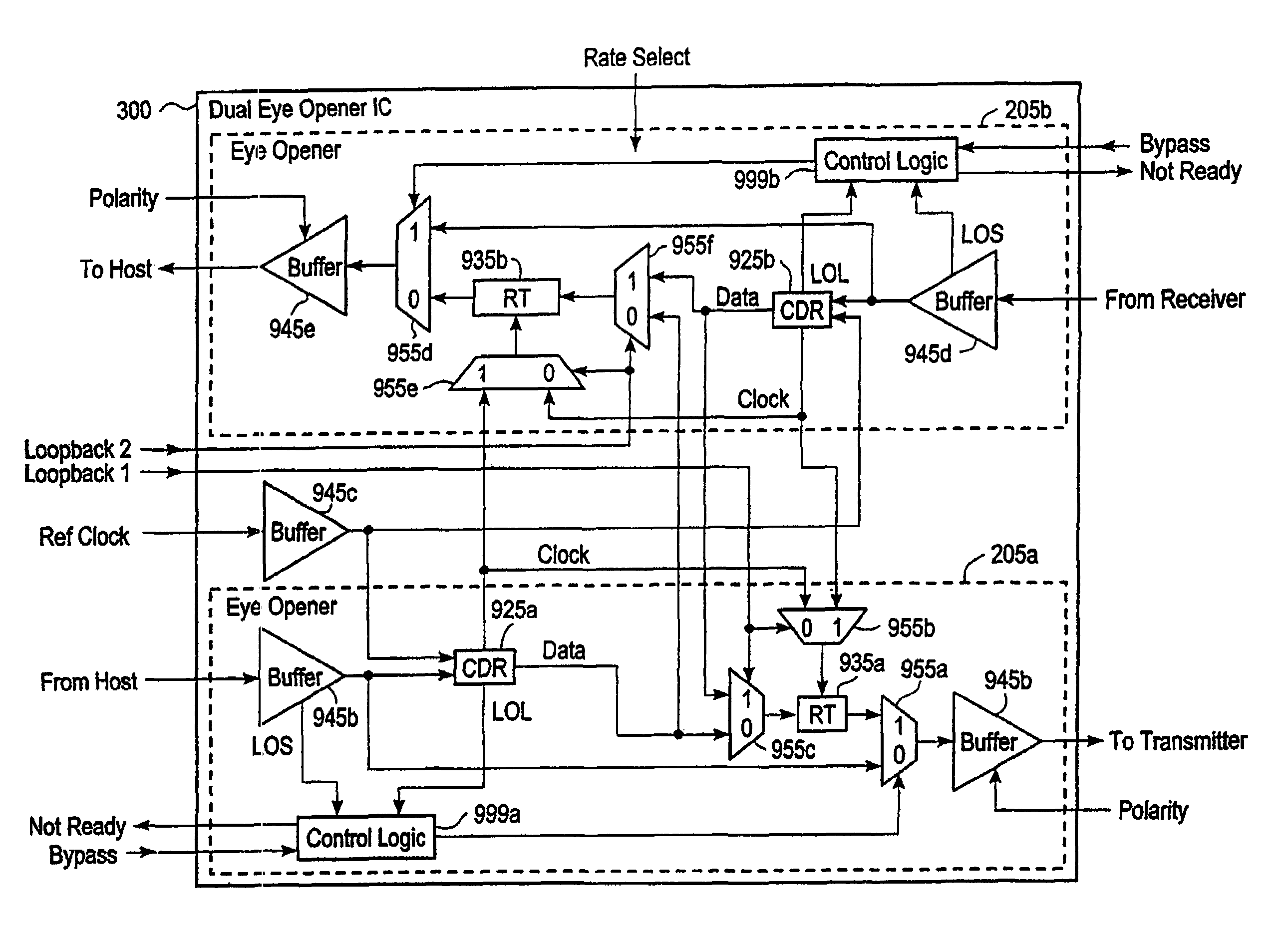
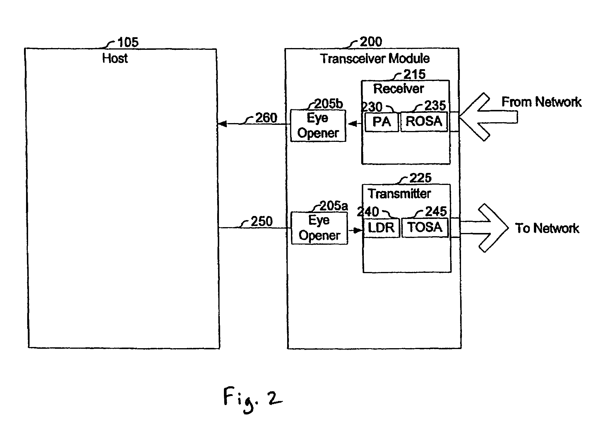
[0013]The present invention overcomes the limitations of the prior art by providing a transceiver module with eye diagram opening functionality for reducing jitter. In one implementation, an optical transceiver module has a serial electrical interface with an electrical output port and an electrical input port. The module also has a receive path and a transmit path. The receive path includes an optical input port, a receiver eye opener and the electrical output port of the serial electrical interface. An optical signal is received by the module at the optical input port. The receiver eye opener retimes and reshapes a serial electrical data stream based on the received optical signal. The retimed and reshaped serial electrical data stream is transmitted from the module via the electrical output port. The transmit path includes the electrical input port of the serial electrical interface, a transmitter eye opener and an optical output port. A second serial electrical data stream is received by the module at the electrical input port. The transmitter eye opener retimes and reshapes the received serial electrical data stream. An optical signal based on the retimed and reshaped serial electrical data stream is transmitted from the module via the optical output port.
[0014]In one implementation, the receiver eye opener and the transmitter eye opener are implemented in a single integrated circuit. The integrated circuit may also include none, some or all of the following: digital to analog converters for example for converting received digital signals to analog control signals, a bypass module for example for bypassing the eye opener(s) under certain conditions, loopback data paths for example for performing diagnostic tests, bit error rate (BERT) tester, adaptive equalizer(s) for example for conditioning the serial data streams, power amplifier or other components for the receiver, driver (e.g., laser driver) or other components for the transmitter, a control module and / or a serial control interface for controlling the circuitry. The integrated circuit may also include various power down or reduced power modes in order to conserve energy. In another aspect, the data path(s) may include two or more eye openers, each suited for a different data rate. Switching between the eye openers permits the accommodation of different data rates.

Problems solved by technology

Reflections caused by discontinuities within a transmission line and amplitude degradations caused by nodes within a path (e.g., wire bond, solder bump, etc.) may significantly increase errors within the signal and increase jitter beyond an acceptable threshold or budget.
Additionally, inductance is proportionally more severe at higher frequencies.
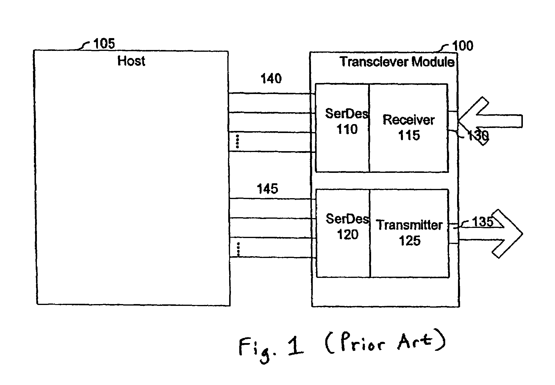
One drawback of module 100 is that the SERDES 110, 120 and the interfaces to the parallel buses 140, 145 require a relatively large amount of space on the transceiver module 100.
Additionally, SERDES consume power and release a relatively large amount of heat.
Another drawback of module 100 is that conventional transceiver modules do not include convenient, cost-effective means to monitor the status of data paths and confirm proper operation of the transceiver.
However, at data rates approaching or exceeding 10 Gb / s, the bit periods become sufficiently short so that signal degradations are difficult to minimize using conventional approaches to serial modules.
Additionally, serial modules at data rates lower than 10 Gb / s can have digital or analog monitoring functions, but the types of error monitoring or diagnostic features that are possible in a module incorporating an integrated SERDES have not thus far implemented.

Method used


Image

  • Integrated circuit with dual eye openers
  • Integrated circuit with dual eye openers
  • Integrated circuit with dual eye openers

Examples


first embodiment

[0094]FIG. 21A illustrates an eye opener having an equalizer. The data path of eye opener 2100 comprises an equalizer 2120, which receives data from a buffer 2105a and outputs data to a buffer 2105b. The buffer 2105a receives data from a receiver and the buffer 2105b sends data to a host. In another embodiment, the buffer 2105a receives data from the host and the buffer 2105b sends data to a transmitter. In one embodiment the eye opener 2100 conditions a signal in bypass mode.

[0095]The equalizer 2120 resets the data path's jitter budget by reshaping and retiming the data to remove channel noise from sources such as inter-symbol interference. The equalizer 2120 is coupled to receive signals representing coefficients from a coefficient module 2110 and a clock signal from a CDR 2130. The equalizer 2120 is preferably an adaptive equalizer that adapts to channel conditions such as changing temperature, but in other embodiments, the equalizer 2120 may be a passive equalizer. Other embodim...

second embodiment

[0098]FIG. 21B illustrates an eye opener having an equalizer. In this embodiment, the data path of eye opener 2180 comprises an equalizer 2150 in series with a CDR 2160 coupled with an RT 2170. The equalizer 2150 receives data from the buffer 2155a and the RT 2170 outputs data to the buffer 2155b. The CDR 2160 and equalizer 2150 may be disposed on separate chips or an integrated circuit. One advantage of this embodiment, is that the signal is conditioned by both the equalizer 2150 and CDR 2160, leading to a lower bit error rate.

[0099]In contrast to the embodiment of FIG. 21A, the equalizer 2150 preferably reshapes and outputs an analog signal by removing channel effects. The equalizer 2150 receives a clock signal from the CDR 2160 to clock the equalizer's digital components.

[0100]The CDR 2160 and RT 2170 retime and reshape the equalized data. The RT 2170 receives a clock signal recovered by the CDR 2160. The CDR 2160 and RT 2170 may comprise the variations discussed herein.

[0101]In ...


PUM


Abstract

A transceiver module having integrated eye diagram opening functionality for reducing jitter is described. The transceiver module may include a transmitter eye opener and a receiver eye opener integrated in a single circuit. The transceiver module may also include serial control and various other integrated components. Other functionalities that may be integrated on the transceiver module include loopback modes, bypass features, bit error rate testing, and power down modes.

Description

CROSS-REFERENCE TO RELATED APPLICATIONS[0001]This application is a divisional of U.S. patent application Ser. No. 10 / 420,027, “Transceiver Module and Integrated Circuit With Dual Eye Openers,” filed Apr. 17, 2003, which claims the benefit of U.S. Provisional Patent Application Ser. No. 60 / 410,509, filed Sep. 13, 2002 and which also claims the benefit of U.S. Provisional Patent Application Ser. No. 60 / 391,877, filed Jun. 25, 2002. The foregoing patent applications are incorporated herein by reference in their entirety.BACKGROUND[0002]A. Technical Field[0003]The present invention relates generally to ensuring data integrity within a networking box, and more particularly, to on-chip clock and data recovery in a transceiver module.[0004]B. Background of the Invention[0005]The proliferation and significance of networking technology is well known. The ever-increasing demand for network bandwidth has resulted in the development of technology that increases the amount of data traveling acro...

Claims


Application Information

Patent Timeline
Patent Type & Authority Patents(United States)
IPC IPC(8): H04B1/38H04B10/24H04L7/033H04L25/24
CPCH04B10/40H04L25/242H04L7/033
Inventor ARONSON, LEWIS B.HOFMEISTER, RUDYMADDEN, CHRISTOPHERFARLEY, MARKCASE, DANLENOSKY, TOM
Owner II VI DELAWARE INC
Why Eureka
Try Eureka