Defect-free semiconductor templates for epitaxial growth

a technology of epitaxial growth and defects, applied in the direction of crystal growth process, semiconductor laser, nanoinformatics, etc., can solve the problems of limiting or even ruining reducing their mobility, and limiting the performance of many semiconductor devices, and achieve high temperature stability

Inactive Publication Date: 2006-09-05
INNOLUME
View PDF44 Cites 96 Cited by
  • Summary
  • Abstract
  • Description
  • Claims
  • Application Information

AI Technical Summary

Benefits of technology

[0021]A method for fabrication of defect-free epitaxial layers on top of a surface of a first defect-containing solid state material includes the steps of selective deposition of a second material, having a high temperature sta

Problems solved by technology

Propagating defects, including threading dislocations, screw dislocations, stacking faults, and antiphase boundaries, play a negative role in semiconductor devices, often limiting or even ruining their performance.
Propagating defects can act as strong scattering centers for carriers, thus reducing their mobility and limiting the performance of many semiconductor devices.
Propagating defects can also act as centers of non-radiative recombination, thus ruining performance of light-emitting devices like light emitting diodes (LED), optical amplifiers, and semiconductor diode lasers.
During device operation, particularly at elevated temperatures

Method used


Image

  • Defect-free semiconductor templates for epitaxial growth
  • Defect-free semiconductor templates for epitaxial growth
  • Defect-free semiconductor templates for epitaxial growth

Examples


Embodiment Construction

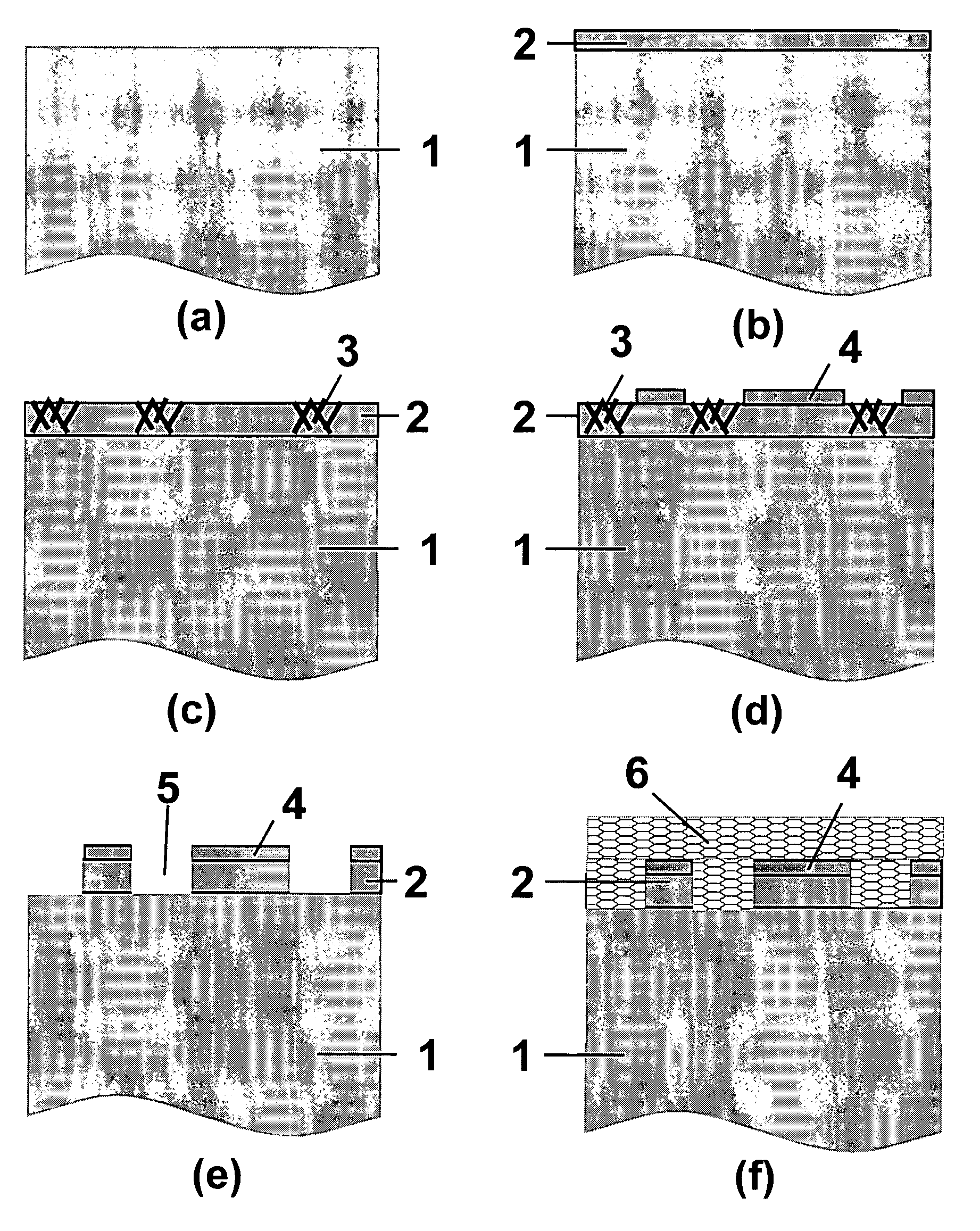
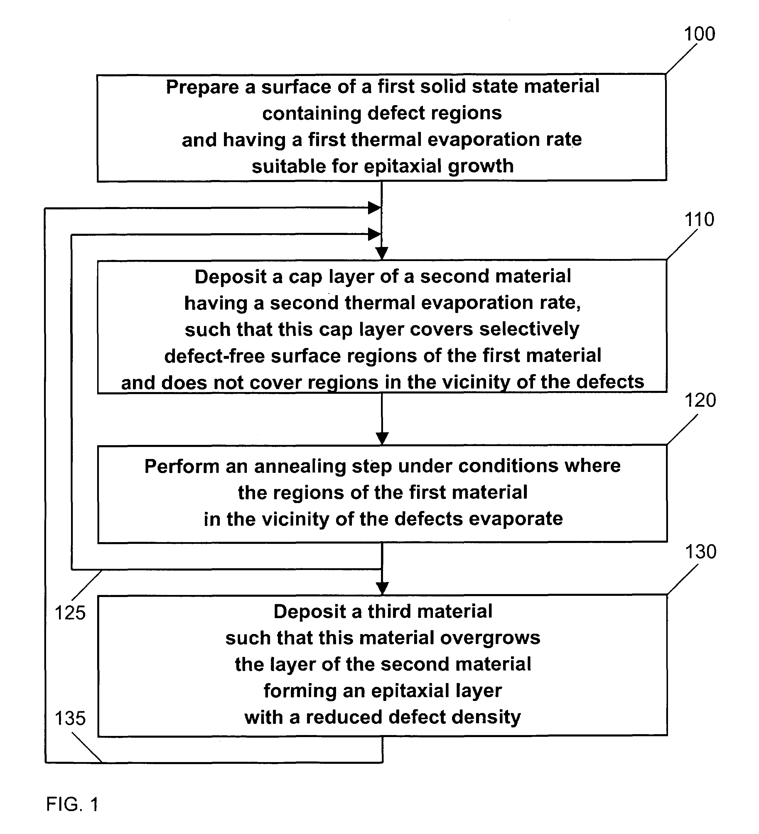
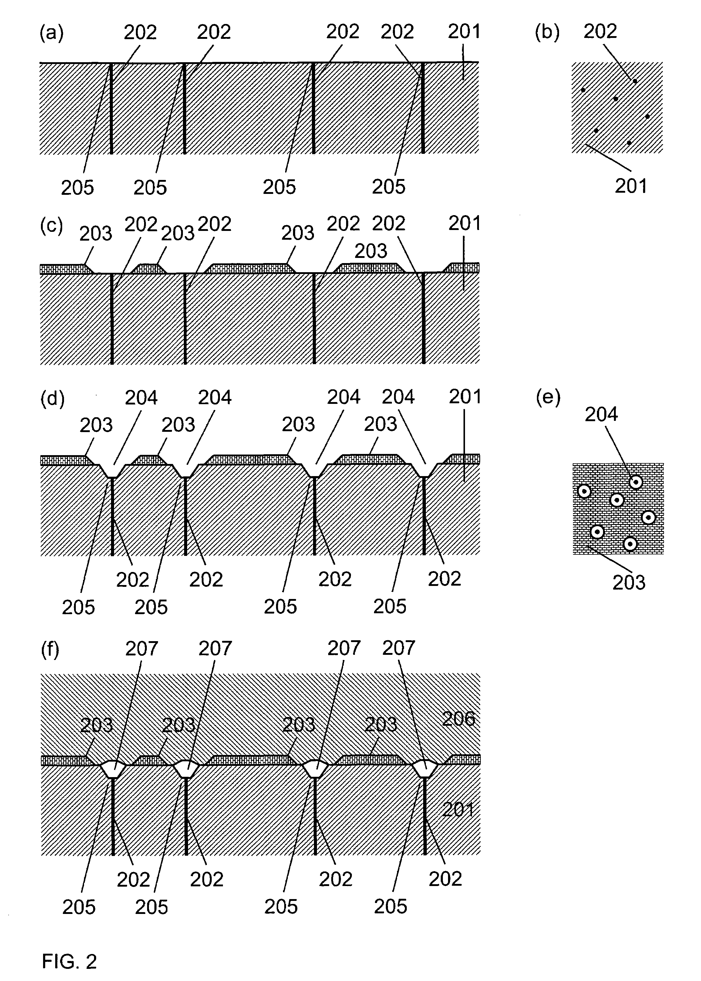
[0055]The current invention overcomes the shortcomings of the prior art with an improved method for selective etching off of defect-rich regions and application of the method to different materials systems and different semiconductor devices.

[0056]One method to eliminate defects in epitaxial layers deposits a temperature stable material, which does not cover the regions in the vicinity of the defects. After thermal treatment, the regions near the defects were evaporated. A mechanism for the selective repulsion of the cap material with respect to the defect regions is additionally disclosed. This is elastic repulsion due to different lattice constants in local plastically-relaxed regions in the vicinity of the dislocation in the epilayer and the cap layer, which has a lattice parameter in no-strain state close to that on the surface of the defect-free regions of the epilayer.

[0057]Referring to FIGS. 9 and 10, the method of in-situ fabrication of dislocation-free structures from plast...


PUM


Abstract

A semiconductor device includes at least one defect-free epitaxial layer. At least a part of the device is manufactured by a method of fabrication of defect-free epitaxial layers on top of a surface of a first solid state material having a first thermal evaporation rate and a plurality of defects, where the surface comprises at least one defect-free surface region, and at least one surface region in a vicinity of the defects, the method including the steps of selective deposition of a second material, having a high temperature stability, on defect-free regions of the first solid state material, followed by subsequent evaporation of the regions in the vicinity of the defects, and subsequent overgrowth by a third material forming a defect-free layer.

Description

REFERENCE TO RELATED APPLICATIONS[0001]This is a divisional of U.S. patent application Ser. No. 10 / 456,377, filed Jun. 6, 2003 now U.S. Pat. No. 6,784,074, entitled DEFECT-FREE SEMICONDUCTOR TEMPLATES FOR EPITAXIAL GROWTH AND METHOD FOR MAKING SAME, which is a continuation-in-part of U.S. patent application Ser. No. 09 / 851,730, filed May 9, 2001, entitled “SEMICONDUCTOR DEVICE AND METHOD OF MAKING SAME”, now U.S. Pat. No. 6,653,166. The aforementioned applications are hereby incorporated herein by reference.BACKGROUND OF THE INVENTION[0002]1. Field of the Invention[0003]The invention pertains to the field of semiconductor devices. More particularly, the invention pertains to fabricating defect-free epitaxial layers for semiconductor device applications.[0004]2. Description of Related Art[0005]Propagating defects, including threading dislocations, screw dislocations, stacking faults, and antiphase boundaries, play a negative role in semiconductor devices, often limiting or even ruini...

Claims


Application Information

Patent Timeline
IPC IPC(8): H01L29/00H01L21/205C30B25/18H01L21/20H01L21/203H01L21/324H01L25/00H01L33/00H01S5/02H01S5/187H01S5/32H01S5/323
CPCB82Y10/00B82Y30/00C30B25/18H01L21/0237H01L21/02381H01L21/02389H01L21/02395H01L21/02439H01L21/0245H01L21/02458H01L21/02463H01L21/02502H01L21/02505H01L21/02507H01L21/02521H01L21/02532H01L21/0254H01L21/02546H01L21/02636H01L21/02639H01L21/02647H01L21/0265H01L21/3245B82Y20/00Y10S438/902H01L33/0062H01S5/3201H01S2301/173H01S2304/12Y10S438/962
Inventor SHCHUKIN, VITALYLEDENTSOV, NIKOLAI
Owner INNOLUME
Why Eureka
Try Eureka