

Thin film transistor array panel for display and manufacturing method thereof
- Summary
- Abstract
- Description
- Claims
- Application Information
AI Technical Summary
Benefits of technology
Problems solved by technology
Method used
Image

Examples
first embodiment
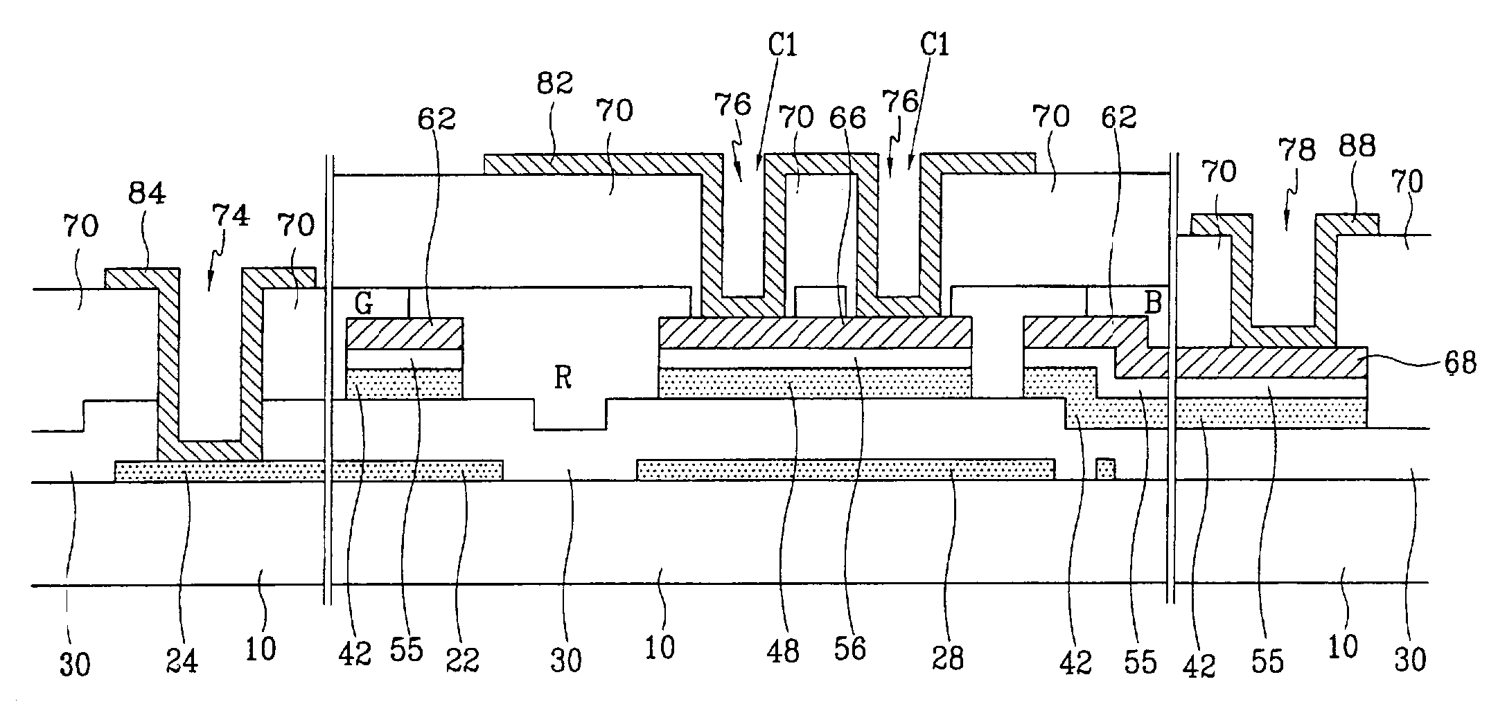
[0065]Now, a method of manufacturing a TFT array panel for an LCD according to the present invention will be described in detail with reference to FIGS. 3A to 7B and FIGS. 1 and 2.
[0066]FIGS. 3A, 4A, 5A, 6A and 7A are layout views of a TFT array panel for a LCD in the respective steps of a manufacturing method thereof according to an embodiment of the present invention, and FIGS. 3B, 4B, 5B, 6B and 7B are sectional views of the TFT array panel shown in FIGS. 3A, 4A, 5A, 6A and 7A taken along the lines IIIB–IIIB′, IVB–IVB′, V–V′, VIB–VIB′ and VIIB–VIIB′, respectively.
[0067]First, as shown in FIGS. 3A and 3B, a plurality of gate lines 22 including a plurality of gate electrodes 26 is formed on a glass substrate 10 by photo etch.
[0068]Next, as shown FIGS. 4A and 4B, after sequentially depositing a gate insulating layer 30, an amorphous silicon layer, and a doped amorphous silicon layer, the doped amorphous silicon layer and the amorphous silicon layer are photo-etched to form a plurali...
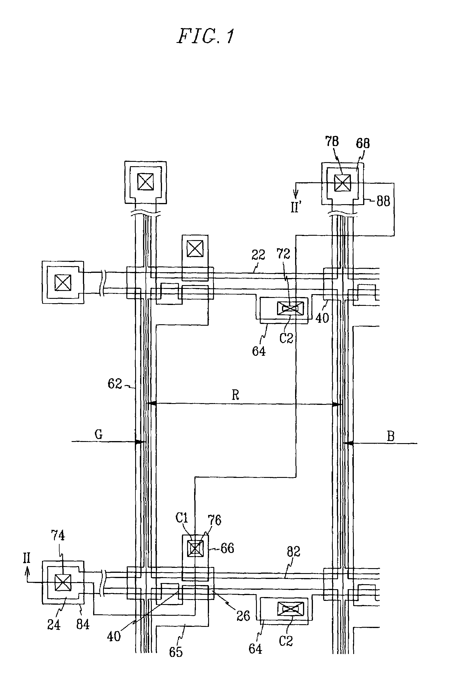
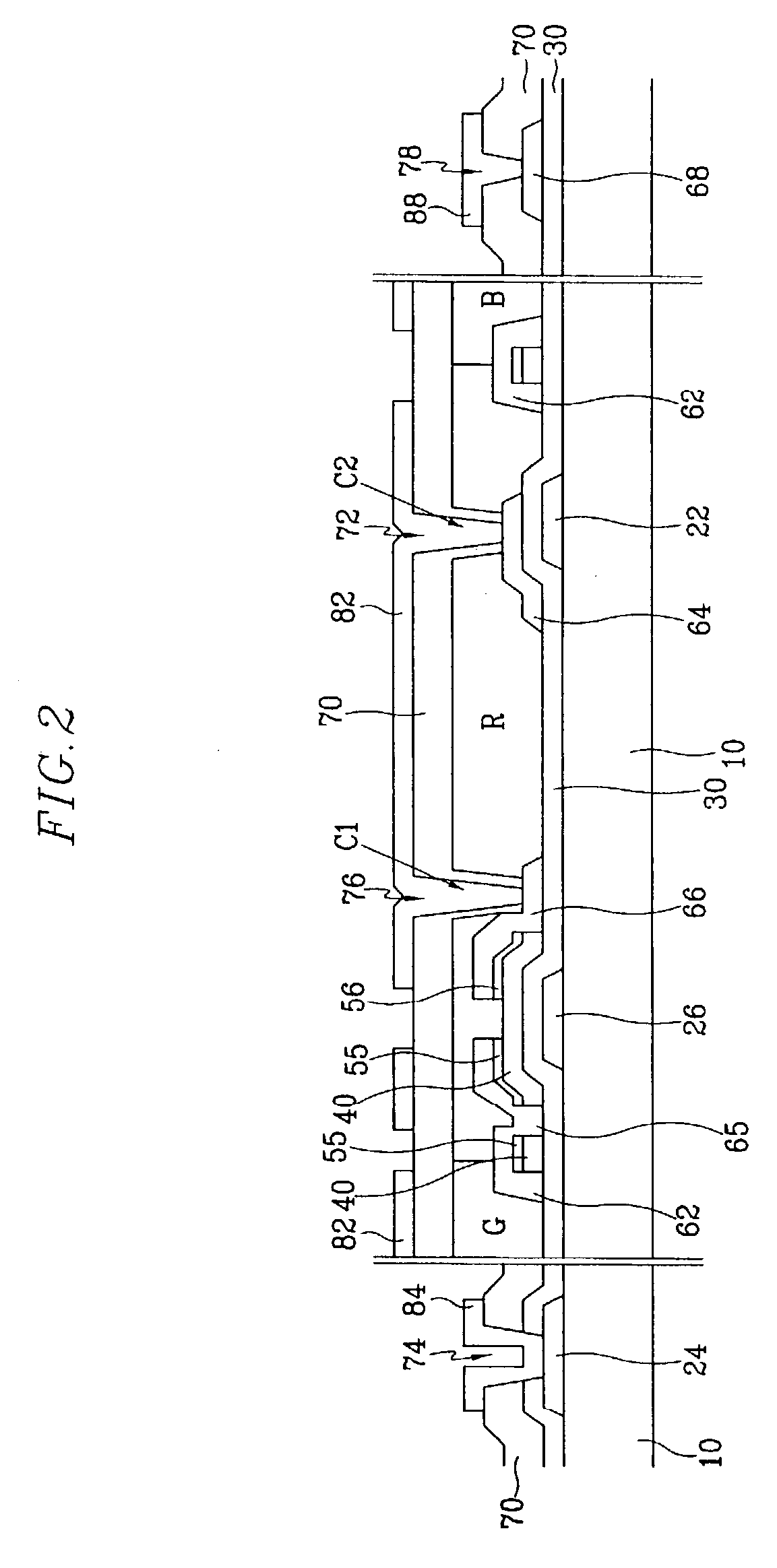
second embodiment
[0077]As shown in FIGS. 8–10, a TFT array panel according the present invention includes a plurality of storage electrode lines 28 formed on an insulating substrate 10 instead of expansions of a plurality of gate lines 22. The storage electrode lines 28 include the same layer as the gate lines 22, extend substantially parallel to the gate lines 22 and electrically separated from the gate lines 22. The storage electrode lines 28 are applied with a predetermined voltage such as a common voltage, and overlap a plurality of drain electrodes 66, which are connected to a plurality of pixel electrodes 82, via the gate insulating layer 30 to form storage capacitors. The storage electrode lines 28 may be omitted if the storage capacitance due to the overlapping of the gate lines 22 and the pixel electrodes82 are sufficient.
[0078]A plurality of semiconductor stripes and islands 42 and 48 and a plurality of ohmic contacts 55, 56 and 58 are provided.
[0079]The semiconductor stripes 42 have almos...
PUM
 Abstract
Description
Claims
Application Information