Semiconductor booster circuit having cascaded MOS transistors

a booster circuit and mos transistor technology, applied in the direction of electric variable regulation, process and machine control, instruments, etc., can solve the problems of complex manufacturing process, inability to suppress the increase of the threshold voltage vt due to the substrate effect, and inability to obtain the desired output voltage vsub>pout /sub>, etc., to achieve the effect of reducing the threshold voltage of the mos transistor and reducing the level of the output voltag

Inactive Publication Date: 2006-09-05
NIPPON STEEL CORP
View PDF12 Cites 21 Cited by
  • Summary
  • Abstract
  • Description
  • Claims
  • Application Information

AI Technical Summary

Benefits of technology

[0024]It is therefore an object of the present invention to provide a semiconductor booster circuit in which a desired output voltage is capable of being obtained, even in the case where a level of a power supply voltage is low, without the necessity of the complicated manufacturing process.
[0037]In the second aspect of the present invention, in order to drive the MOS transistors to perform the boosting operation, other clock signals are employed which are different from the clock signals which are used to drive the stages and have a larger amplitude than the power supply voltage, whereby it is possible to secure the threshold for conducting the MOS transistor and also it is possible to prevent the reduction of the output voltage due to the substrate effect.
[0043]In addition, the gate voltage of the MOS transistor which operates to perform the boosting operation in the stages is controlled by the clock signals other than the source voltage and the drain voltage, and the amplitude of each of the clock signals is made larger than the input power supply voltage of the booster circuit, whereby since even in the employment of the low power supply voltage, the MOS transistor can be sufficiently rendered to an on state, and also the voltage drop due to the threshold voltage of the MOS transistor is eliminated so that the boosting capability is improved.
[0053]In the fourth aspect of the present invention, since the substrate portions of the MOS transistors constituting the booster circuit are divided into groups and the potentials of the substrate portions in the respective groups are controlled independently of one another, the potentials at the substrate portions of the MOS transistors of each group can be fixed to a potential different from that of another group. Therefore, it is possible to suppress the increase of the threshold voltage of the MOS transistor due to the substrate bias effect, and also the level of the output voltage can be made higher than that in the conventional booster circuit.

Problems solved by technology

That is, in the conventional booster circuit; there arises a problem that in the case where the level of the power supply voltage Vdd is low, the desired output voltage VPOUT can not be obtained even if the number n of stages of the booster circuit is set to any large value.
However, in this configuration as well, the increase of the threshold voltage Vt due to the substrate effect can not be suppressed.
As a result, the manufacturing process becomes complicated.
This is a disadvantage.
This problem becomes especially pronounced during the low power source voltage operation in which the margin between the threshold voltage Vt and the power supply voltage Vdd is small.
Therefore, there arises a problem that the potential of the source terminal of the MOS transistor, which is located in the more backward stage, becomes higher, and the difference in the potential between the source terminal and the substrate portion is increased so that due to the so-called substrate bias effect, the threshold voltage Vt is increased, and hence the output voltage VPOUT is limited due to the increase of the threshold voltage Vt.

Method used


Image

  • Semiconductor booster circuit having cascaded MOS transistors
  • Semiconductor booster circuit having cascaded MOS transistors
  • Semiconductor booster circuit having cascaded MOS transistors

Examples


first embodiment

[0077]the present invention will hereinafter be described in detail with reference to FIGS. 1 to 10.

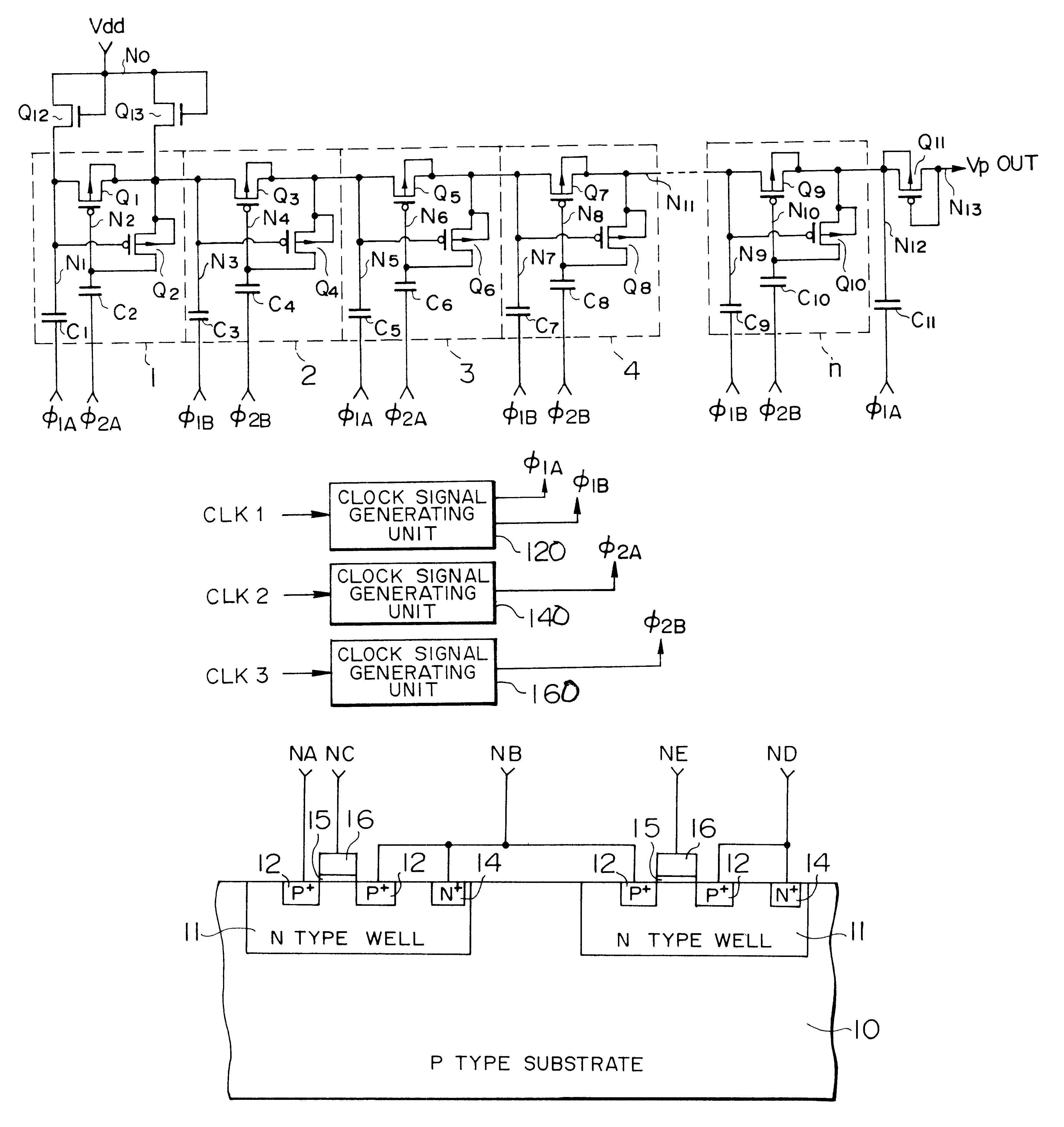
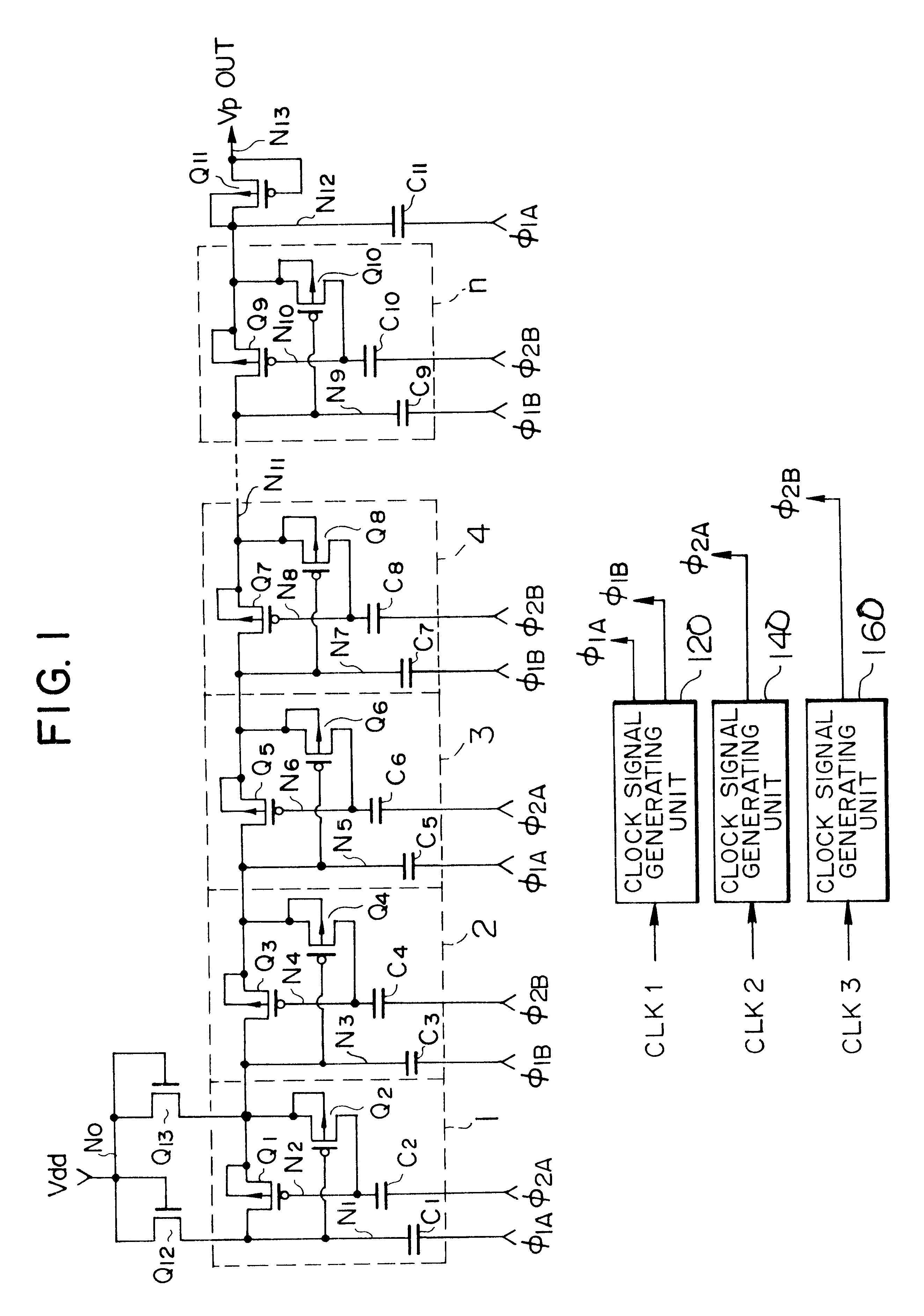
[0078]FIG. 1 shows a configuration of a semiconductor booster circuit according to the first embodiment of the present invention.

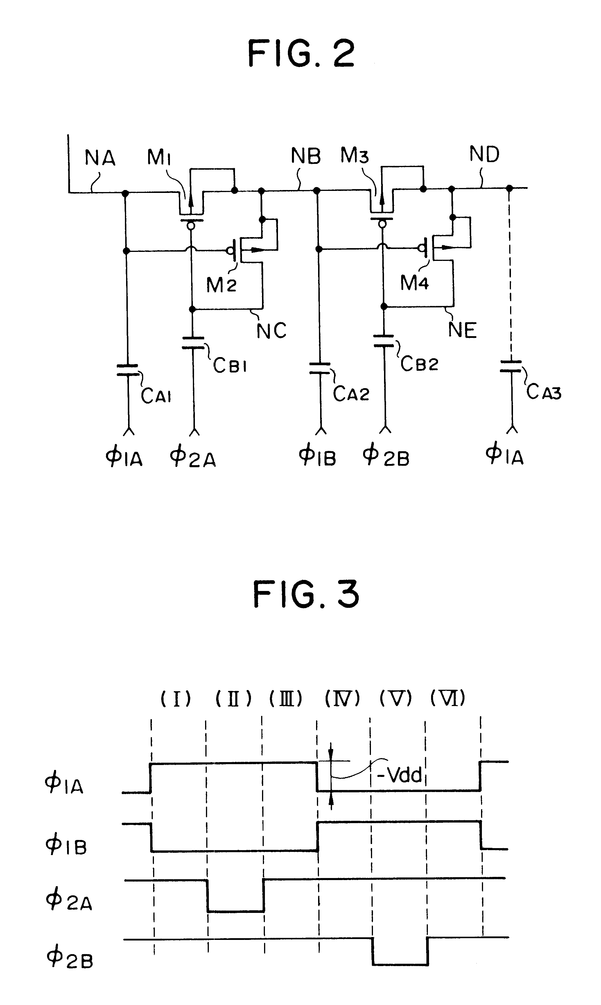
[0079]As shown in FIG. 1, n elements of P-channel MOS transistors Q1, Q3, Q5, Q7, . . . , Q9 are connected in cascade to configure a booster circuit having n stages. Substrate portions of the transistors Q1, Q3, Q5, Q7, . . . , Q9 are electrically insulated from one another and also are connected to source terminals of the transistors Q1, Q3, Q5, Q7, . . . , Q9, respectively. In addition, to drain terminals (represented by nodes N1, N3, N5, N7, . . . , N9) a clock signal φ1A or φ1B which is shown in FIG. 3 is inputted through respective capacitors C1, C3, C5, C7, . . . , C9.

[0080]In addition, to gate terminals (represented by nodes N2, N4, N6, N8, . . . , N10) of the transistors Q1, Q3, Q5, Q7, . . . , Q9, a clock signal φ2A or φ2B which is shown in FIG. 3 i...

second embodiment

[0136]Next, the description will hereinbelow be given with respect to a semiconductor booster circuit according to the present invention with reference to FIGS. 7 and 8.

[0137]FIG. 7 is a circuit diagram showing a configuration of the semiconductor booster circuit according to the second embodiment of the present invention.

[0138]In FIG. 7, n elements of P-channel MOS transistors Q30 to Q34 are connected in cascade to configure a booster circuit having n stages. Substrate portions of the respective transistors Q30 to Q34 are electrically insulated from one another, and also gate terminals and the substrate portions are connected to respective source terminals N31 to N35. Then, a clock signal φA or φB which is shown in FIG. 8 is inputted to the source terminals N30 to N35 through capacitors C30 to C35, respectively.

[0139]In the booster circuit of the present embodiment, as an inputted signal, the power supply voltage Vdd is inputted from a source terminal N37 of a P-channel MOS transis...

third embodiment

[0145]Next, the description will hereinbelow be given with respect to a semiconductor booster circuit according to the present invention with reference to FIGS. 9 and 10.

[0146]FIG. 9 is a circuit diagram showing a configuration of the semiconductor booster circuit according to the third embodiment of the present invention.

[0147]In FIG. 9, N-channel MOS transistors Q40 to Q44 are connected in cascade to configure the booster circuit having n stages. Substrate portions of the respective transistors Q40 to Q44 are electrically insulated from one another, and also the substrate portions and gate terminals are connected to respective source terminals N40 to N44. Then, the clock signal φA or φB which is the same as that shown in FIG. 8 is inputted to the terminals N40 to N44 through capacitors C40 to C44, respectively.

[0148]In the booster circuit according to the present embodiment, the power supply voltage Vdd is inputted as an input signal from a source terminal N47 of an N-channel MOS ...


PUM


Abstract

The semiconductor booster circuit includes a plurality of stages, each of which has a MOS transistor and two capacitors. The MOS transistor, having a drain, a source and a gate, is formed in a well of a substrate portion. One capacitor has a terminal connected to the drain of the MOS transistor, while the other capacitor has a terminal connected to the gate of the MOS transistor. A first clock signal generating means generate a first clock signal via another terminal of one capacitor. A second clock signal generating mean s generate a second clock signal, with a larger amplitude than a power supply voltage, via another terminal of another capacitor. The plurality of stages are cascaded together, and in each of the stages the source of the MOS transistor is electrically connected to the well in which the transistor is formed, while the wells are electrically insulated from each other.

Description

BACKGROUND OF THE INVENTION[0001]1. Field of the Invention[0002]The present invention relates to a semi-conductor booster circuit and more particularly to a semiconductor booster circuit, such as a charge pump circuit, which is used in an EEPROM (Electrically Erasable and Programmable Read Only Memory) and a flash memory.[0003]2. Description of the Related Art[0004]In recent years, along with the promotion of a single 5V power supply or the promotion of a single 3V power supply for semiconductor integrated circuits such as EEPROMs and flash memories, the boosting has been performed in the integrated circuit. As a result, semiconductor booster circuits such as a Cockcroft Walton circuit and a charge pump circuit have been employed.[0005]FIG. 18 shows a configuration of a conventional semiconductor booster circuit.[0006]As shown in the figure, N-channel MOS transistors Q20 to Q24 are connected in cascade to configure a booster circuit having n stages. The gate terminals of the transis...

Claims


Application Information

Patent Timeline
Patent Type & Authority Patents(United States)
IPC IPC(8): G05F3/02H02M3/07
CPCH02M3/073H02M2003/078H02M2003/076H02M2003/075H02M3/075H02M3/076H02M3/078G11C5/14
Inventor SAWADA, KIKUZOSUGAWARA, YOSHIKAZU
Owner NIPPON STEEL CORP
Why Eureka
Try Eureka