

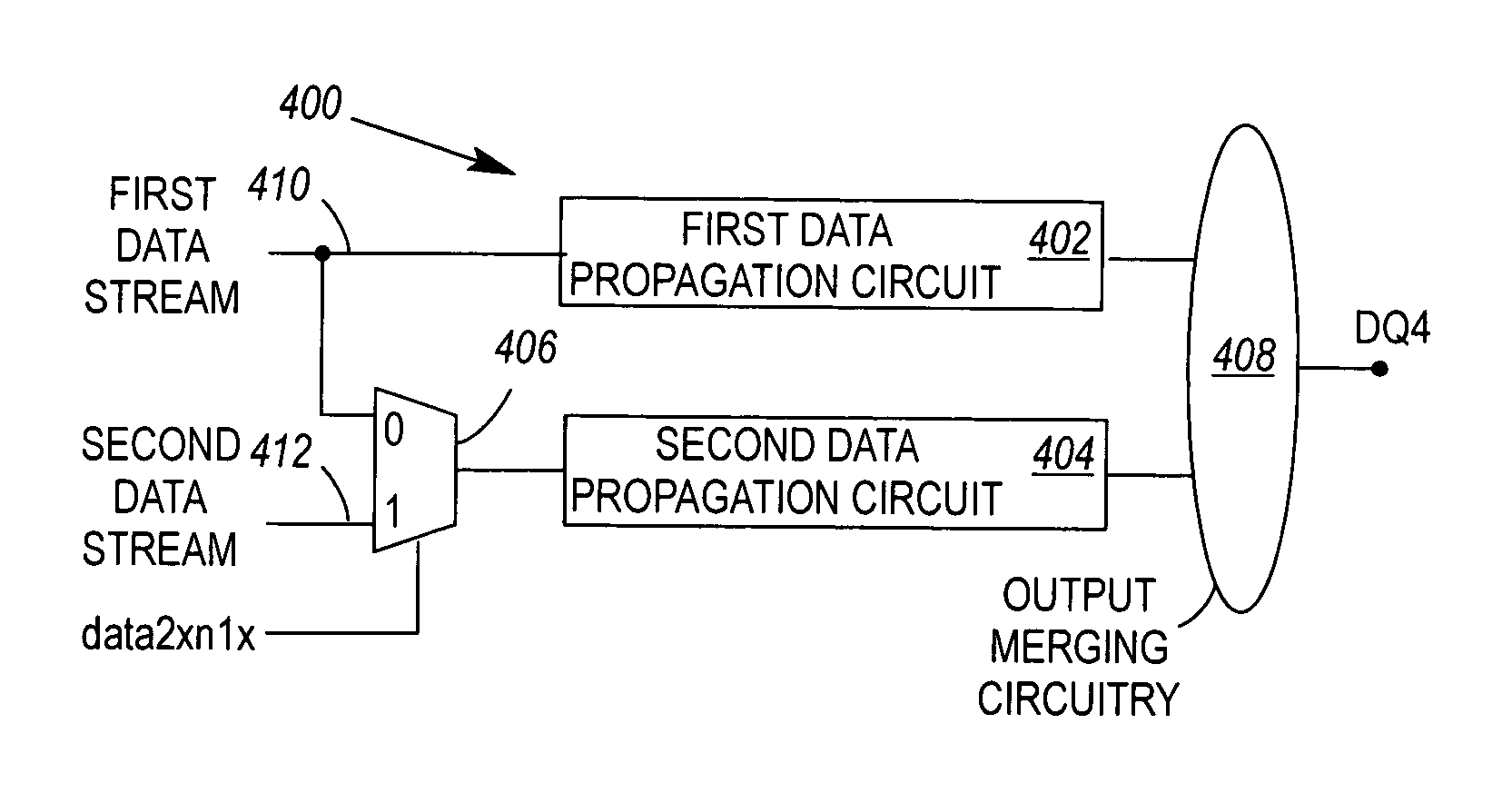
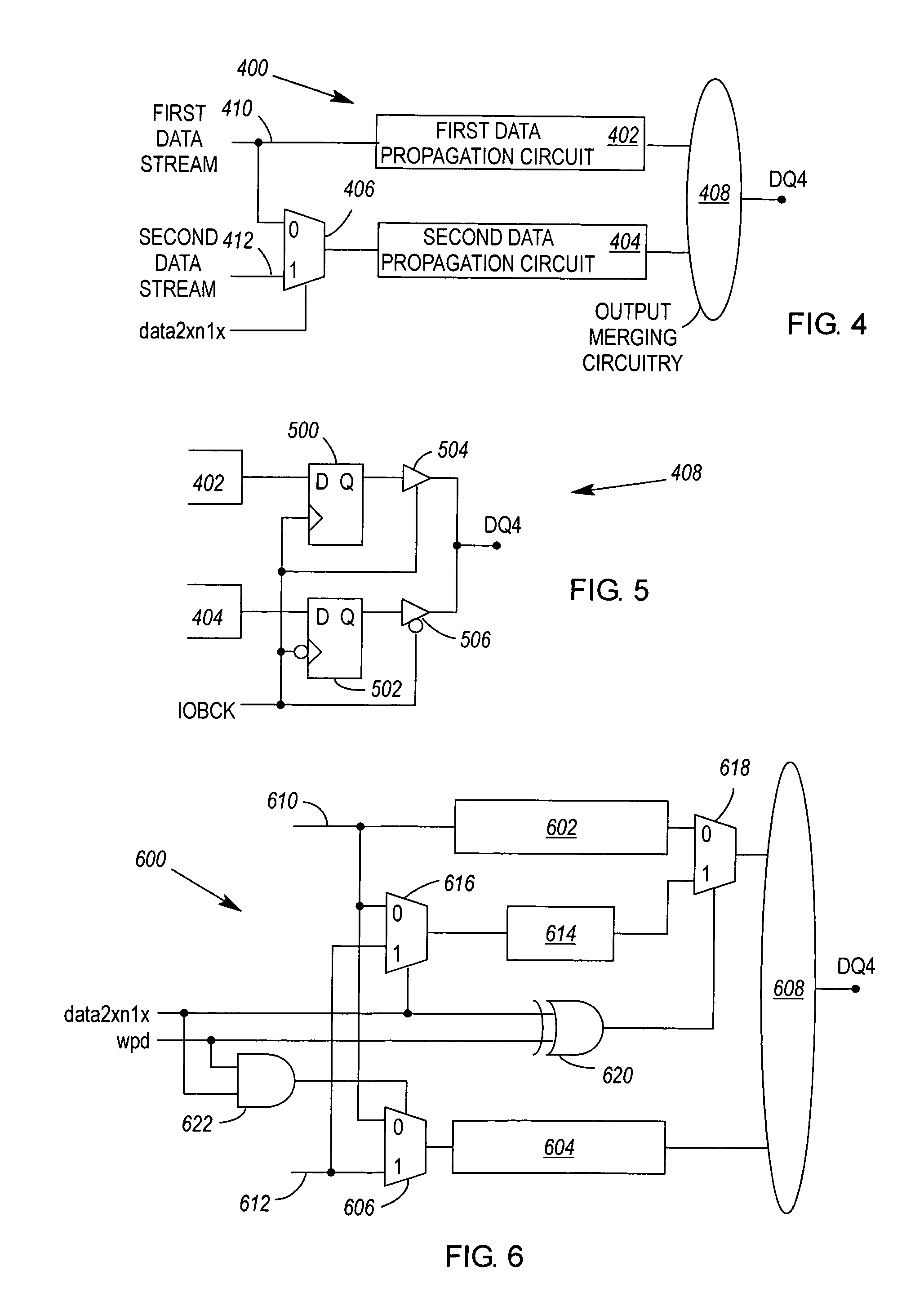
Memory controller driver circuitry having a multiplexing stage to provide data to at least N-1 of N data propagation circuits, and having output merging circuitry to alternately couple the N data propagation circuits to a data pad to generate either a 1x or Mx stream of data
a memory controller and driver circuit technology, applied in the field of memory controllers, can solve the problems of high cost of memory controller design, development and verification, and achieve the effect of saving time and expens
- Summary
- Abstract
- Description
- Claims
- Application Information
AI Technical Summary
Benefits of technology
Problems solved by technology
Method used
Image

Examples
Embodiment Construction
1. In General: a Memory Controller with a Greater Number of Functional Modes
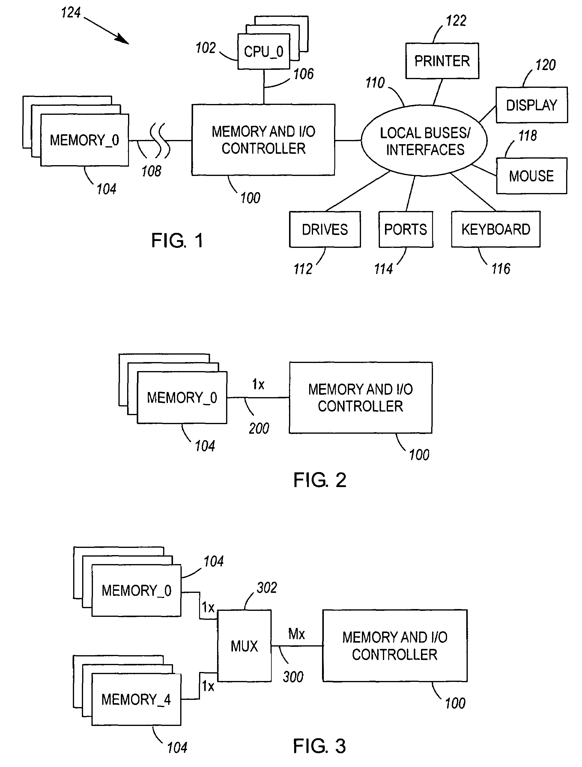
[0038]A memory controller 100 with a greater number of functional modes is illustrated in FIGS. 1–3. The memory controller 100 is preferably a double data rate (DDR) memory controller, but need not be. A DDR memory controller 100 is one which is capable of communicating with DDR synchronous dynamic random access memories (SDRAMs). See, e.g., JEDEC Standard No. 79 published June 2000, which is hereinafter referred to as the “JEDEC DDR SDRAM Specification” (and which is hereby incorporated by reference).
[0039]FIG. 1 illustrates an exemplary computer system 124 in which the memory controller 100 may be used. The computer system 124 comprises a number of central processing units 102 (CPUs) which are connected to the memory controller 100 over a system bus 106. As shown in FIG. 1, the memory controller 100 preferably forms part of an integrated memory and input / output (I / O) controller (MIOC) 100. The MIOC 100 rec...
PUM
 Abstract
Description
Claims
Application Information