Semiconductor device having SOI construction

a semiconductor device and soi technology, applied in the field of semiconductor devices, can solve the problems of increasing wiring resistance, enlarge the overall increasing the size of the package, and reducing the noise of the device, so as to achieve the effect of small dimensions, low noise performance and reduced device nois

Active Publication Date: 2006-09-12
DENSO CORP
View PDF12 Cites 9 Cited by
  • Summary
  • Abstract
  • Description
  • Claims
  • Application Information

AI Technical Summary

Benefits of technology

[0010]In view of the above-described problem, it is an object of the present invention to provide a semiconductor device having small dimensions and low noise performance.
[0012]In the above device, the third semiconductor layer embedded in the trench fixes the electric potential of the first semiconductor layer disposed on the backside of the semiconductor substrate. Therefore, the noise of the device can be reduced. Further, the third semiconductor layer is provided by a vertical type construction so that the device has small dimensions. Thus, the device has small dimensions and low noise performance.
[0014]Preferably, the first semiconductor layer has a first conductive type, the second semiconductor layer has a second conductive type, and the third semiconductor layer has the first conductive type with an impurity concentration higher than the first semiconductor layer. More preferably, the part of the second semiconductor layer surrounded by the trench further includes a diffusion layer disposed inside of the first insulation film so that the diffusion layer surrounds the part of the second semiconductor layer. The diffusion layer has the second conductive type with an impurity concentration higher than the part of the second semiconductor layer. The second electrode on the second insulation layer connects to the diffusion layer through the contact hole. Furthermore preferably, the third semiconductor layer, the first insulation film and the diffusion layer provide a first capacitor. In this case, the diffusion layer is used for one electrode of the first capacitor so that the impurity concentration of the second semiconductor layer can be reduced. Therefore, semiconductor elements and the like can be formed and integrated in the second semiconductor layer so that the dimensions of the device are reduced.
[0015]Preferably, the device further includes a fourth semiconductor layer disposed between the insulation layer and the second semiconductor layer. The fourth semiconductor layer has the second conductive type with an impurity concentration higher than the second semiconductor layer. The fourth semiconductor layer contacts the diffusion layer. More preferably, the fourth semiconductor layer, the insulation layer and the first semiconductor layer provide a second capacitor. In this case, the fourth semiconductor layer is used for one electrode of the second capacitor so that the impurity concentration of the second semiconductor layer can be reduced. Therefore, semiconductor elements and the like can be formed and integrated in the second semiconductor layer so that the dimensions of the device are reduced.
[0016]In the above cases, the impurity concentration of the third semiconductor layer in the trench can be controlled appropriately so that the third semiconductor layer is used for a resistor. This resistor and the above capacitors can reduce the noise of the device. Further, the resistor and the capacitors are provided by a vertical type construction so that dimensions of the device are small. Therefore, the device has small dimensions and low noise performance.
[0018]In the above device, the noise of the device can be reduced. Further, the third semiconductor layer is provided by a vertical type construction so that the device has small dimensions. Thus, the device has small dimensions and low noise performance. Further, the trench does not penetrate the insulation layer so that the method for manufacturing the device is simplified.

Problems solved by technology

Semiconductor elements boasting high speeds and high degrees of integration due to SOI technology have had the problem that heat generated during operation cannot be easily radiated outside the semiconductor device due to the presence of substrates having a low thermal conductivity.
For this reason, in the highly integrated high-speed semiconductor devices, such problems easily arise as changes in the element characteristics, increase in wiring resistance, melting of the solder bumps, or peeling of the protective film due to thermal stress.
However, mounting these elements inevitably enlarges the overall size of the package.

Method used


Image

  • Semiconductor device having SOI construction
  • Semiconductor device having SOI construction
  • Semiconductor device having SOI construction

Examples


first embodiment

[0033]The inventors have preliminarily studied about a semiconductor device having a SOI construction.

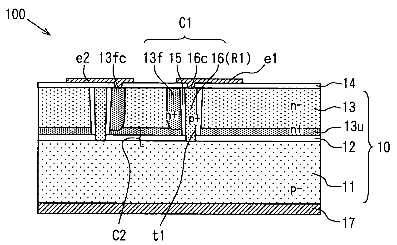
[0034]A semiconductor device 90 shown in FIG. 13 has been studied. FIG. 13 is a typical cross section showing the semiconductor device 90 in a state in which a flip chip is mounted on a wiring board 70 with solder bumps 71 interposed between them.

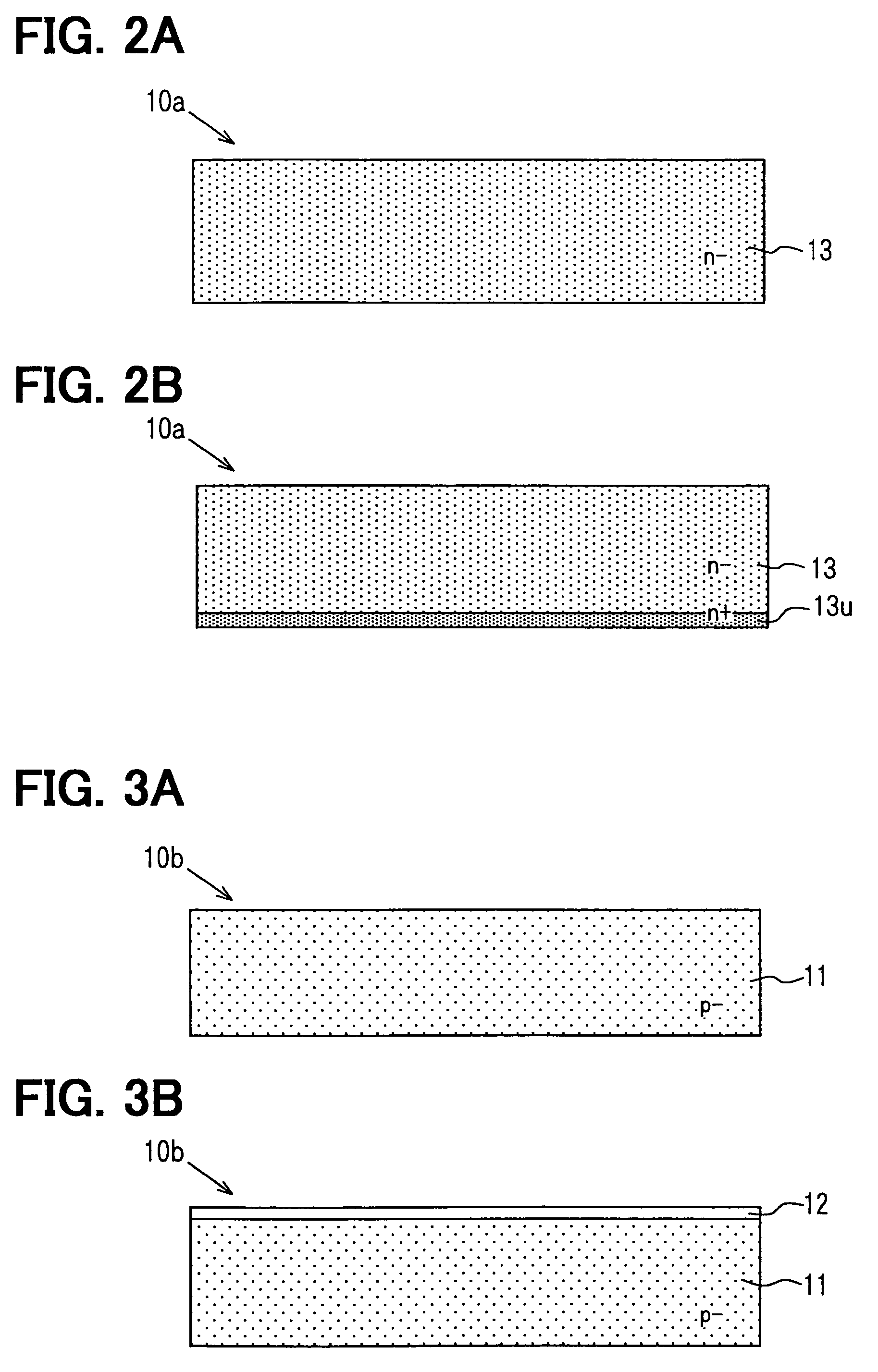
[0035]The semiconductor device 90 shown in FIG. 13 employs a semiconductor board with an SOI structure having a buried insulation film 92. A first semiconductor layer 91 and a metallic layer 94 are formed on the backside (the upper side in FIG. 13) of the buried insulation film 92. A second semiconductor layer 93 is formed on the main side (the lower side in FIG. 13) of the buried insulation film 92, with semiconductor elements formed in the second semiconductor layer 93. Heat generated in the semiconductor elements is radiated through the metallic layer 94 formed on the first semiconductor layer 91. This allows for a semiconductor device w...

second embodiment

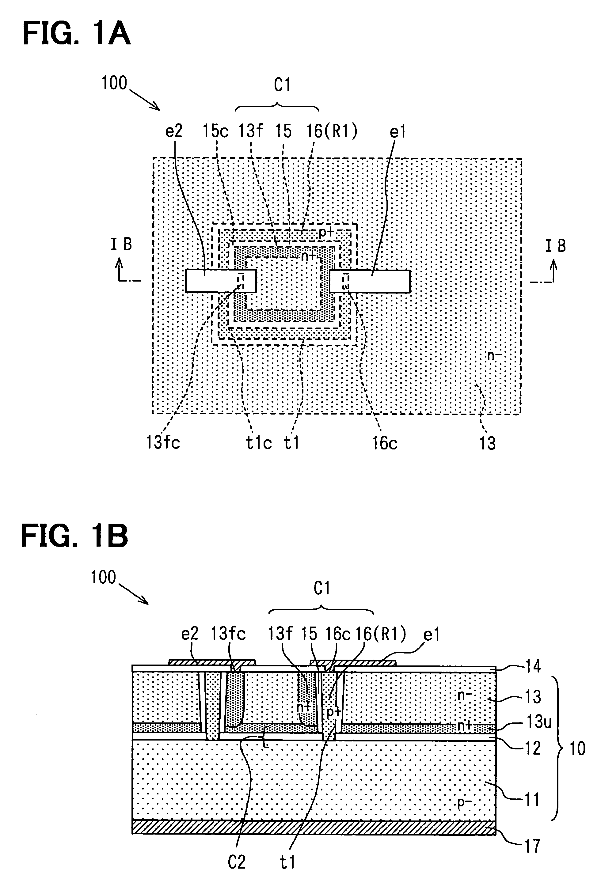
[0068]Each of the semiconductor devices 100–102 according to the first embodiment has one trench in the form of a closed ring in plan view. The trench is formed on the main side of a semiconductor board having an SOI structure. Each of these semiconductor devices 100–102 also has a capacitor employing a sidewall insulation film in its trench. A semiconductor device according to a second embodiment of the present invention has a first trench similar to the foregoing trench and a second trench. The second trench takes the form of a closed ring in plan view and is formed inside the first trench. This embodiment will be described below with reference to the drawings.

[0069]FIGS. 9A and 9B typically show the semiconductor device 103 according to this embodiment. FIG. 9A is a top plan of the semiconductor device 103. FIG. 9B is a cross section taken along line IXB—IXB of FIG. 9A. The same reference numerals are assigned to the similar parts of the semiconductor device 103 and the semicondu...

third embodiment

[0073]Each of the semiconductor devices according to the first embodiment has a capacitor employing a trench sidewall insulation film. Semiconductor devices according to a third embodiment of the present invention have diodes formed in them. This embodiment will be described below with reference to the drawings.

[0074]FIG. 10 is a cross section typically showing a semiconductor device 104 according to this embodiment. The same reference numerals are assigned to the similar parts of the semiconductor device 104 and the semiconductor device 100 shown in FIGS. 1A and 1B.

[0075]The semiconductor device 104 is similar in structure to the semiconductor device 100 shown in FIGS. 1A and 1B, but has another diffusion region 20a of the n-conductive type (n+), which is buried in first semiconductor layer 11 and formed in contact with the adjacent surface of buried insulation film 12. Trench t1 extends to the buried diffusion region 20a. The formation of the buried diffusion region 20a of the n-c...


PUM


Abstract

A semiconductor device includes: a semiconductor substrate including a first semiconductor layer, an insulation layer and a second semiconductor layer, which are laminated in this order; a trench penetrating both of the second semiconductor layer and the insulation layer and reaching the first semiconductor layer; and a third semiconductor layer. The trench has a ring shape on a principal surface of the substrate so that a part of the second semiconductor layer and a part of the insulation layer are surrounded with the trench. The third semiconductor layer is disposed in the trench through a first insulation film disposed on a sidewall of the trench so that the third semiconductor layer contacts the first semiconductor layer at a bottom of the trench.

Description

CROSS REFERENCE TO RELATED APPLICATION[0001]This application is based on Japanese Patent Application No. 2003-394456 filed on Nov. 25, 2003, the disclosure of which is incorporated herein by reference.FIELD OF THE INVENTION[0002]The present invention relates to a semiconductor device having a SOI (i.e., silicon on insulator) substrate, and more particularly to a semiconductor device utilizing a trench sidewall insulation film as a dielectric film of a capacitor.BACKGROUND OF THE INVENTION[0003]SOI (silicon on insulator) technology is employed to achieve semiconductor elements with higher speeds and higher degrees of integration. SOI technology includes the steps of forming a semiconductor layer on an insulation board, and then forming semiconductor elements in the semiconductor layer.[0004]For example, U.S. Pat. No. 6,429,486 discloses a semiconductor device employing a semiconductor board with an SOI structure having a buried insulation film.[0005]FIG. 12 is a cross section of the ...

Claims


Application Information

Patent Timeline
Patent Type & Authority Patents(United States)
IPC IPC(8): H01L29/00H01L27/04H01L21/02H01L21/60H01L21/762H01L21/822H01L21/84H01L23/48H01L23/58H01L27/12H01L29/8605H01L29/861H01L29/94
CPCH01L21/743H01L21/76275H01L21/76286H01L29/8605H01L29/945H01L23/585H01L21/84H01L2224/81801H01L24/81H01L27/1203
Inventor ISHIO, SEIICHIROTAI, AKIRA
Owner DENSO CORP
Why Eureka
Try Eureka