High frequency switch circuit

Inactive Publication Date: 2006-09-12
PANASONIC CORP
View PDF20 Cites 42 Cited by
  • Summary
  • Abstract
  • Description
  • Claims
  • Application Information

AI Technical Summary

Benefits of technology

[0033]This configuration prevents the signal passing through the first through fourth FETs from leaking through the fifth through ninth resistors.
[0034]As described above, according to the high frequency switch circuit according to the invention, a cascade circuit of a plurality of FETs is used, while the electric potential is fixed at the two end points and the respective interm

Problems solved by technology

When such a single FET is used as a switching device, a GaAs-FET has a low insertion loss, but has a difficulty in increasing the isolation.
Nevertheless, the reduction of the gate width causes an increase in the ON resistance, and hence causes the problem of an increase in the insertion loss.
Thus, a low insertion loss and a high isolation are difficult to be achieved simultaneously.
As such, a low insertion loss and a high isolation are difficult to be achieved simultaneously in a single FET.
Nevertheless, in the configuration of such a multistage cascade o

Method used


Image

  • High frequency switch circuit
  • High frequency switch circuit
  • High frequency switch circuit

Examples


embodiment 1

[0046

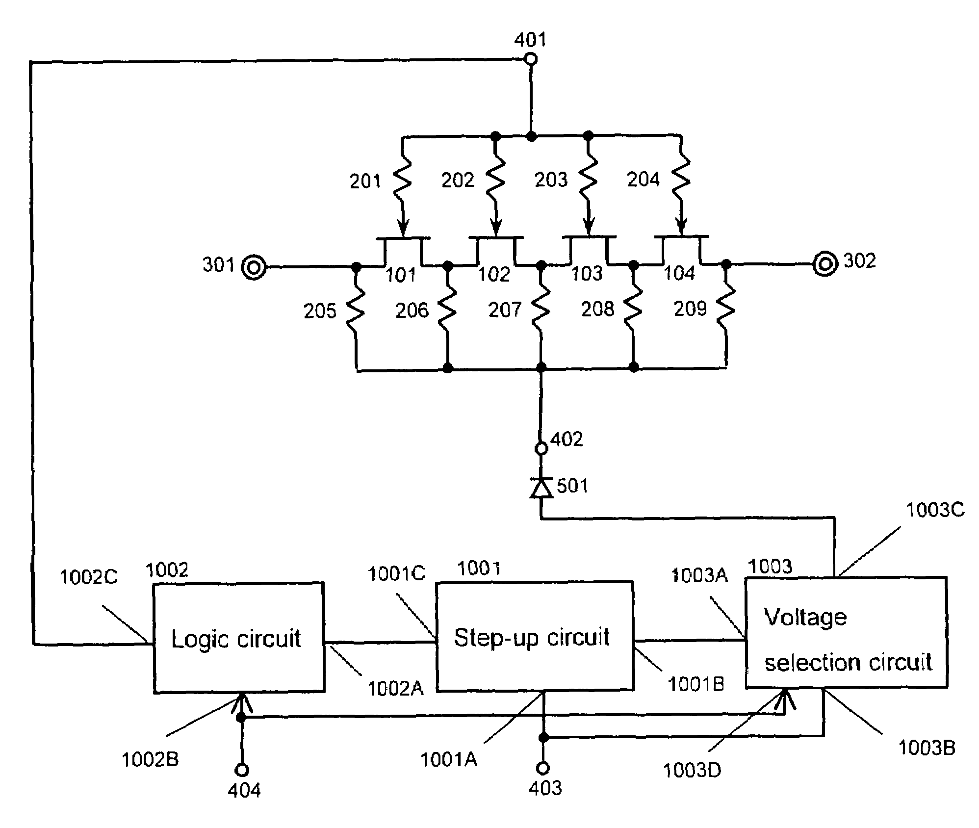
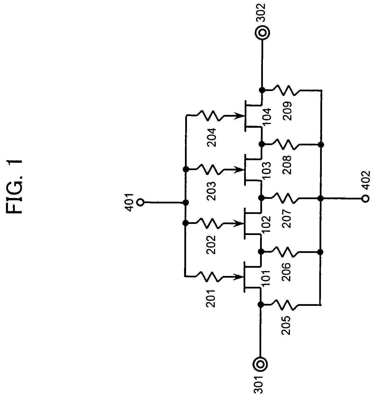
[0047]FIG. 1 is a circuit diagram of a high frequency switch circuit according to Embodiment 1 of the invention. In FIG. 1, numerals 101–104 indicate first through fourth FETs which are of depression type and cascaded. Numerals 201–204 indicate first through fourth resistors for providing a gate bias to the first through fourth FETs 101–104. Numerals 205–209 indicate fifth through ninth resistors for fixing the source-drain voltage of the first through fourth FETs 101–104. Numeral 301 indicates a first high frequency signal input and output terminal, while numeral 302 indicates a second high frequency signal input and output terminal. Numeral 401 indicates a first control terminal, while numeral 402 indicates a second control terminal.

[0048]The detailed connection relation is described below. The drain terminal of the FET 101 is connected to the source terminal of the FET 102. The drain terminal of the FET 102 is connected to the source terminal of the FET 103. The drain termin...

embodiment 2

[0062

[0063]In a circuit according to the invention, the resistors 205–209 for fixing the electric potential at the two end points and the respective intermediate connection points of the cascade circuit of the FETs 101–104 in Embodiment 1 have a resistance value of 1 kΩ or higher. The upper limit for the resistance value of the resistors 205–209 is not restricted specifically. However, in practice, the resistance value is preferably 1 MΩ or lower, or alternatively 10 MΩ or lower. The resistance value of the resistors 201–204 is set between a few tens kΩ and a few hundred kΩ or the like.

[0064]This configuration prevents the signal passing through the FETs 101–104 from leaking through the resistors 205–209. The other effects are the same as those of Embodiment 1.

embodiment 3

[0065

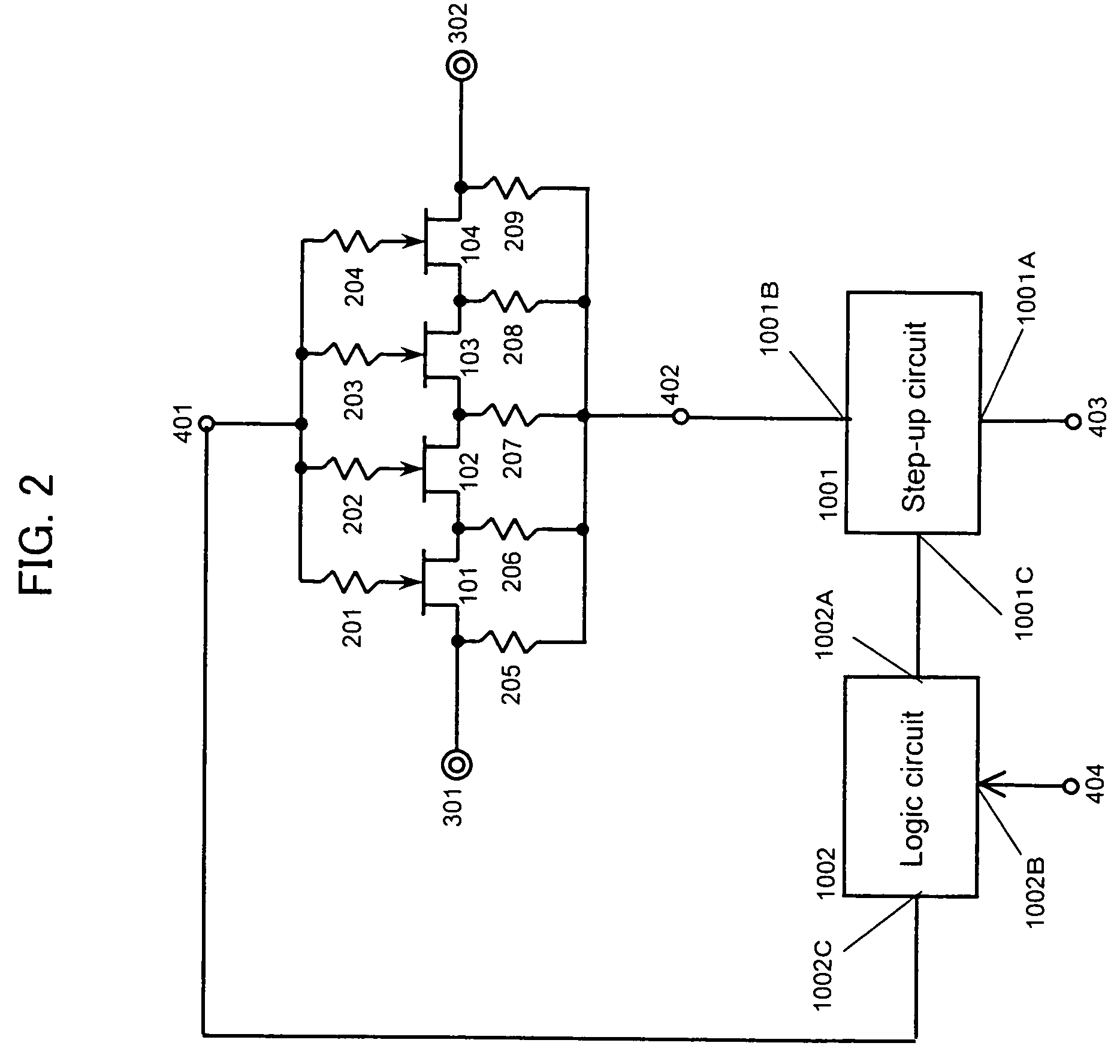
[0066]FIG. 2 is a circuit diagram of a high frequency switch circuit according to Embodiment 3 of the invention. In the previous Embodiment 1, a voltage applied from the outside has been provided intact to the control terminals 401 and 402. In contrast, in the present Embodiment 3, the voltage applied from the outside is stepped up first, and then this stepped-up voltage is provided to the control terminals 401 and 402.

[0067]For this purpose, in the present Embodiment 3, a step-up circuit 1001 and a logic circuit 1002 are added to the configuration of Embodiment 1. At the same time, added are: a control terminal 403 for providing a control voltage therethrough to the step-up circuit 1001; and a control terminal 404 for providing a control voltage therethrough to the logic circuit 1002. The step-up circuit 1001 steps up the voltage applied through the control terminal 403, into a desired voltage by means of a charge pump. The logic circuit 1002 uses the voltage stepped up by the...


PUM


Abstract

One end of each of five resistors is connected to each of the two ends and the respective intermediate points of a cascade of four depression-type FETs, while the other ends of the five resistors are provided with a predetermined voltage. This configuration fixes the source-drain potential of the four FETs. This fixing of the source-drain potential of the FETs permits stable application of a bias voltage for turning ON the FETs between the gate and the source each FET, so as to ensure the ON-OFF switching of the FETs.

Description

BACKGROUND OF THE INVENTION[0001]1. Technical Field[0002]The present invention relates to a high frequency switch circuit built in a switch semiconductor integrated circuit or a communication terminal device. In particular, the invention is preferably applicable in a high frequency switch circuit which needs to have low insertion loss, high isolation, and low distortion characteristics, as well as in a communication terminal device using this switch circuit. This high frequency switch circuit is used, for example, as an antenna switch in a portable phone.[0003]2. Prior Art[0004]In these days, mobile telecommunication business such as in car telephones and portable phones is growing in remarkable rapidness. In many countries in the world, various mobile telecommunication systems have commenced operations. Meanwhile, in these mobile telecommunication systems, semiconductor field effect transistors (FETs) are used widely in signal processing units in major portable terminals. In partic...

Claims


Application Information

Patent Timeline
IPC IPC(8): H03L5/00H03K17/687
CPCH03K17/687H03J2200/29
Inventor HIDAKA, KENICHITARA, KATSUSHINAKATSUKA, TADAYOSHI
Owner PANASONIC CORP
Why Eureka
Try Eureka