[0012]It is therefore an object of the present invention to provide an authentication communicating apparatus in which an encryption key and
control data of the system cannot be obtained even by the monitoring of the external terminal. This prevents a cracker aiming at illegal accesses to the system from analyzing such information as the encryption key and
control data and hence from attacking the illegal
copy protection technique to protect copyrights of digital contents. The authentication communicating apparatus thereby prevents the illegal copy of digital contents.
[0018]In the configuration above, it is difficult to externally obtain or steal internal signals of the
semiconductor chip and a communication command for the authentication process, and an encryption key for the encryption process cannot be tampered to be externally inputted to the authentication communicating device configured in a large scale integration (LSI) chip. It is therefore difficult for the
third person to analyze the authentication process to circumvent the illegal copy (unauthorized
copying) protection technique. This also makes it difficult to circumvent the illegal
copy protection technique by modifying an electronic apparatus. In consequence, there can be implemented an electronic apparatus capable of communicating digital contents requiring copyright protection in quite a safe environment.
[0019]Furthermore, when an electrically rewritable nonvolatile memory is necessary to store inherent information of an electronic device on which the pertinent
semiconductor device is mounted, the memory is also formed on the pertinent same chip. This prevents the inherent information of the electronic device from being intercepted or stolen by a
third person. Since the electrically rewritable nonvolatile memory is employed, security can be improved at a low cost by writing mutually different inherent information items for the respective devices. The information items can be written in the electrically rewritable nonvolatile memory before the installation of the memory in the system.
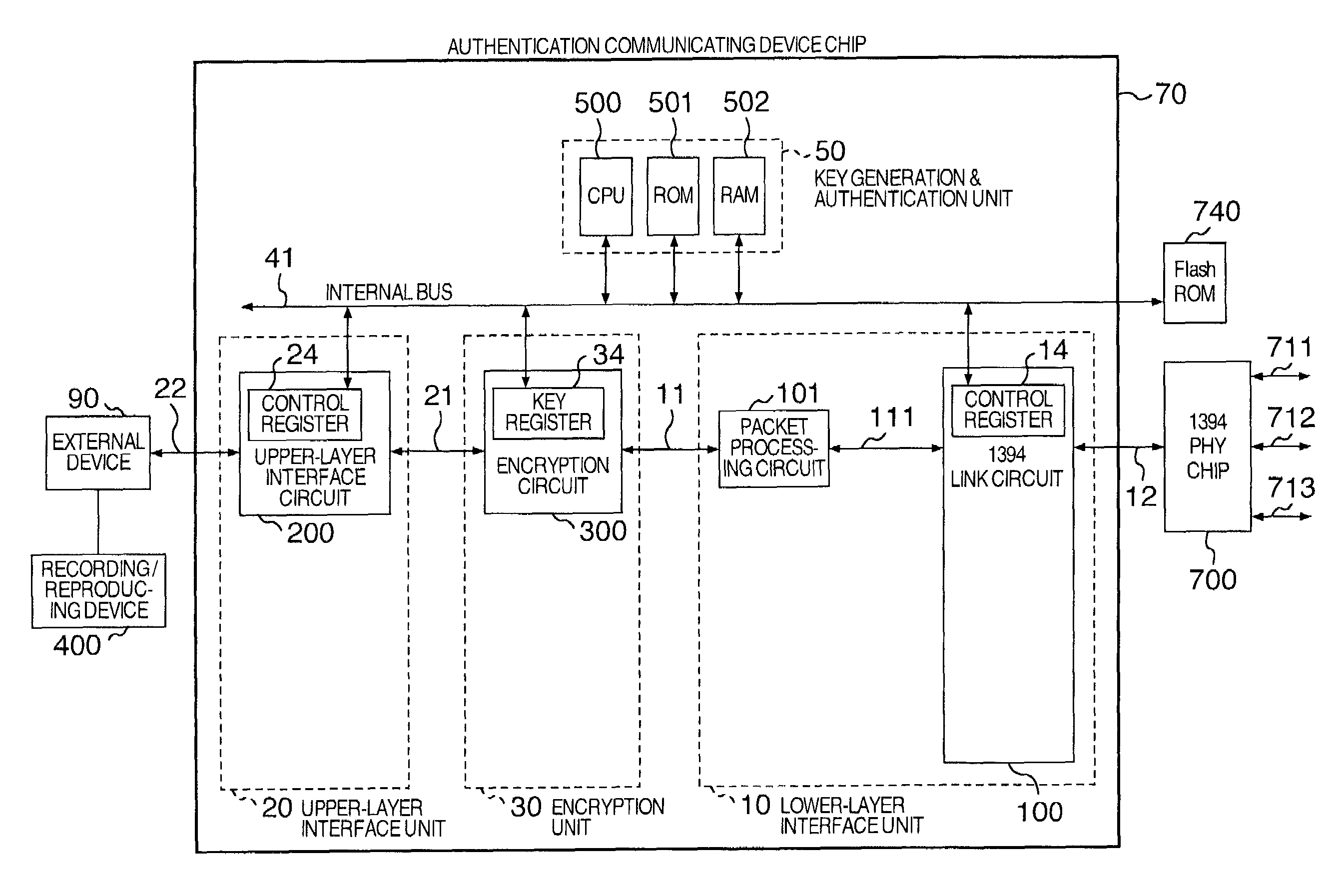
[0020]Additionally, the
main processing unit which generates a key code, which authenticates an external device, and which controls communication; the encryption unit, and the interface unit are mutually connected via an internal bus. When an electrically rewritable nonvolatile memory is necessary to store inherent information of an electronic device on which the pertinent
semiconductor device is mounted, a bus
control circuit is disposed between an external terminal connected to the nonvolatile memory and the internal bus to control a bus change-over operation. Therefore, the encryption process and the authentication process cannot be externally intercepted. This also makes it difficult for a
third person external with respect to the chip to tamper an encryption key used in the encryption process and a
communication control code used in the authentication process. Therefore, neither the encryption key nor the
communication control code can be easily inputted to the system in the illegal way.
Attack from crackers such as analysis of the encryption and authentication and modification of devices can be resultantly prevented. This improves safety against the illegal copy of digital contents for which the copyright protection is required.
[0021]Moreover, there is further required a host CPU to control the overall system of the electronic apparatus on which the semiconductor device is mounted. The main
processing unit of the semiconductor device includes a nonvolatile memory having stored therein a program implementing a
key generation algorithm and an authentication
algorithm to authenticate an external device requesting data communication and program-execution-type control means for generating a key code and for determining approval / non-approval of communication of data with an external device according to the program. In this configuration, there is provided a communication circuit for communication between the control means and the host CPU between a communication port of the host CPU and the internal bus. As a result, this prevents, in a semiconductor device having a communication port to the host CPU, the encryption process and the authentication process from being externally intercepted via the communication port. This also makes it difficult for a third person to externally tamper an encryption key in the encryption process and a
communication control code in the authentication process. Therefore, neither the encryption key nor the communication control code can be easily inputted to the system in the illegal way.
Attack from crackers such as analysis of the encryption and authentication and modification of devices can be resultantly prevented.
[0022]In this case, the
control unit is so configured to accept only restricted and predetermined commands. This prevents illegal intervention in the encryption process and the authentication process and hence improves safety of the system.

