Semiconductor device and power supply system

a technology of magnetic field and power supply system, which is applied in the direction of solid-state devices, pulse techniques, basic electric elements, etc., can solve the problems of large reduction of conversion efficiency and loss of turn-on and turn-off of high-side switches, so as to reduce parasitic inductance, improve voltage conversion efficiency, and reduce gate voltage. the effect of influen

Active Publication Date: 2006-09-19
RENESAS ELECTRONICS CORP
View PDF3 Cites 33 Cited by
  • Summary
  • Abstract
  • Description
  • Claims
  • Application Information

AI Technical Summary

Benefits of technology

[0019]An object of the present invention is to provide a power supply system which is capable of reducing an influence exerted on a gate voltage even when parasitic inductance is large and greatly improving voltage c

Problems solved by technology

A problem arises-in that particularly when the parasitic inductance LsH of the high side switch 51 increases, turn

Method used


Image

  • Semiconductor device and power supply system
  • Semiconductor device and power supply system
  • Semiconductor device and power supply system

Examples


embodiment 1

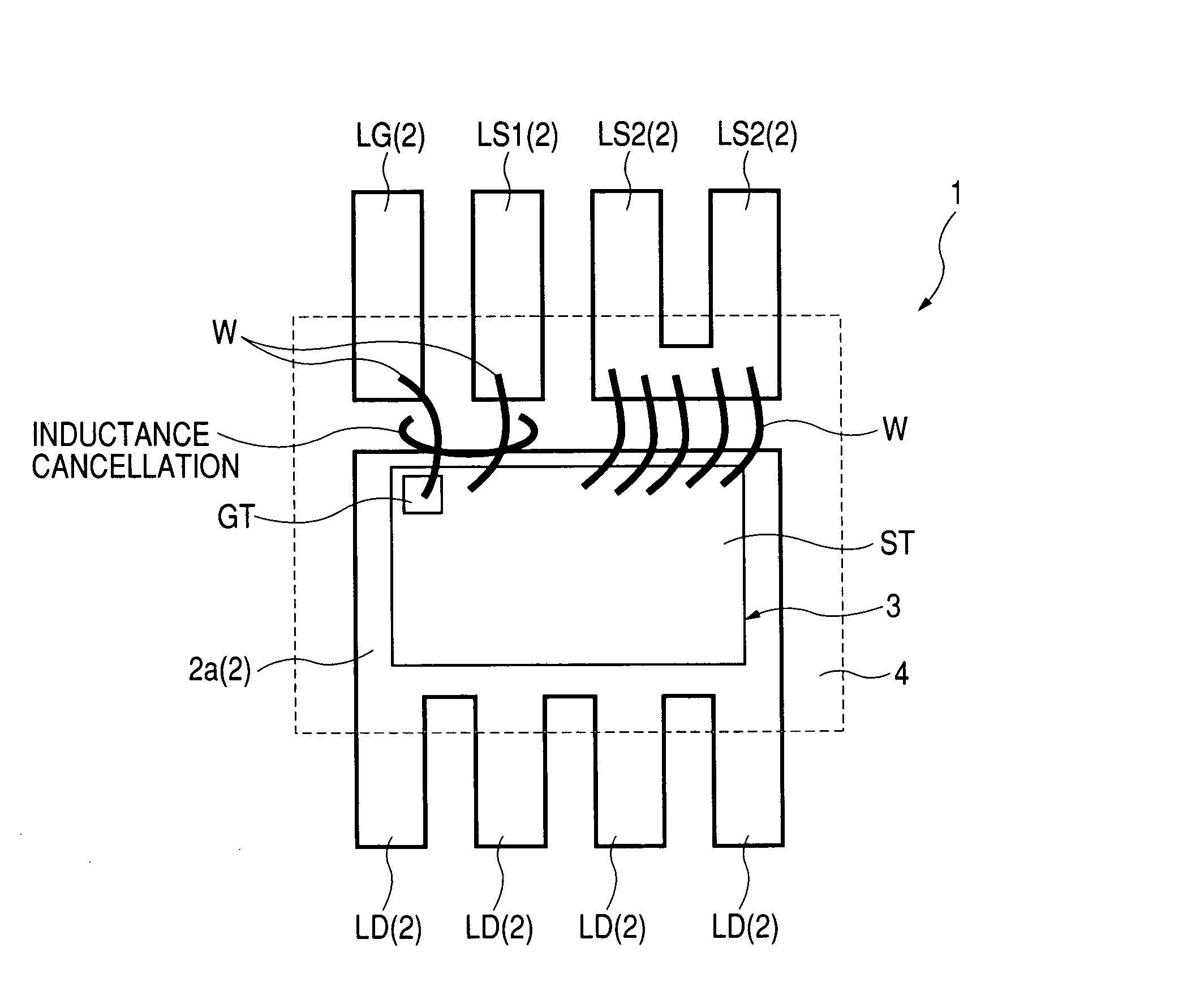
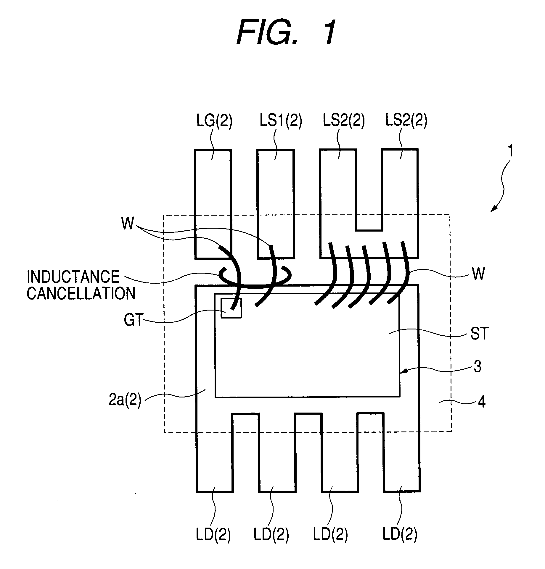
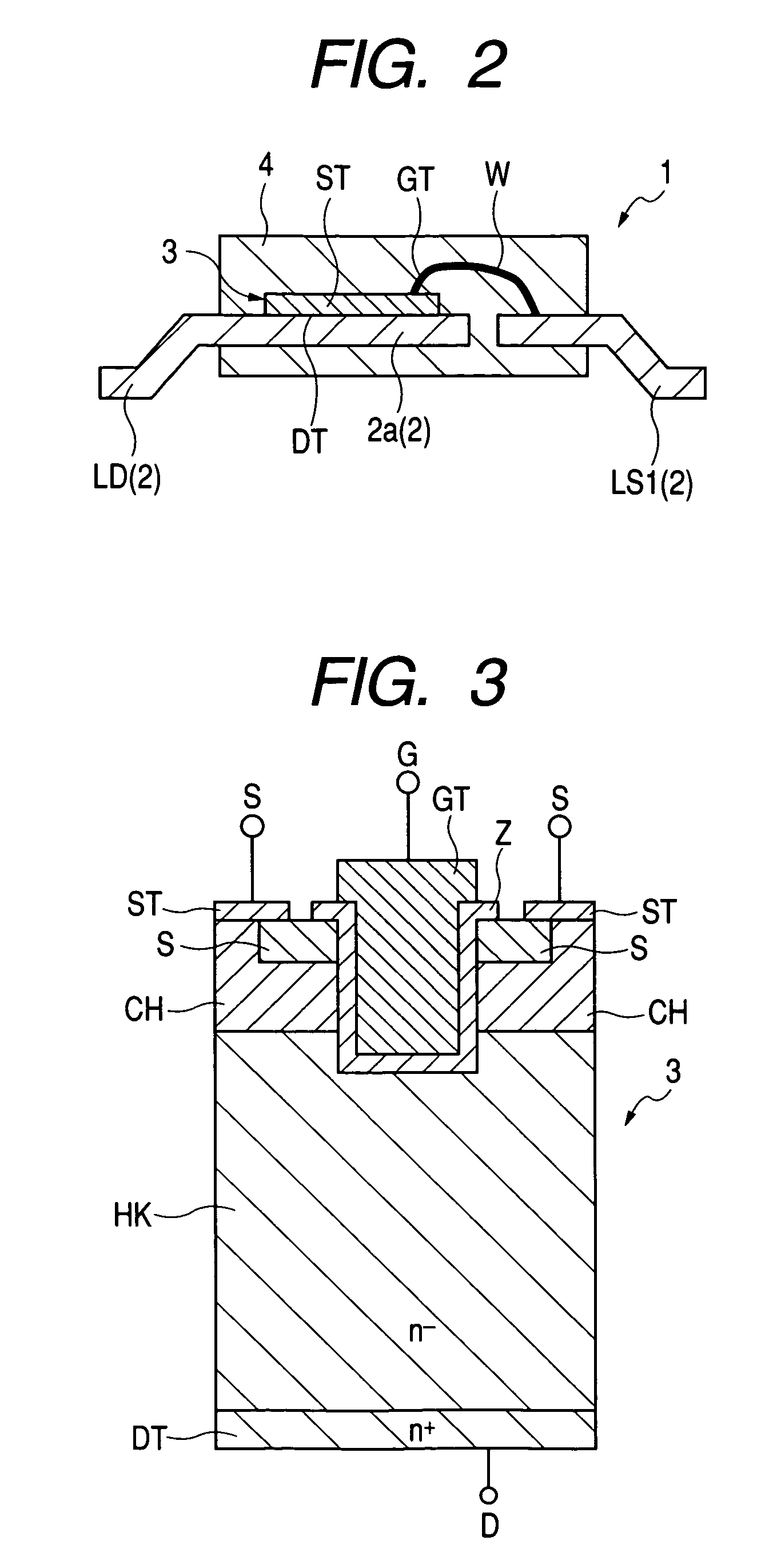
[0053]FIG. 1 is an explanatory view showing one example of a configuration of a power MOS-FET according to an embodiment 1 of the present invention, FIG. 2 is a cross-sectional view of the power MOS-FET shown in FIG. 1, FIG. 3 is an explanatory view illustrating one example of a chip layout in the power MOS-FET shown in FIG. 1, FIG. 4 is an explanatory view showing an example of packaging of a printed wiring board on which a DC / DC converter is configured using the power MOS-FET shown in FIG. 1, FIG. 5 is an equivalent circuit diagram of the DC / DC converter packaged on the printed wiring board shown in FIG. 4, FIG. 6 is an explanatory view showing another configurational example of the power MOS-FET shown in FIG. 1, FIG. 7 is a cross-sectional view of the power MOS-FET shown in FIG. 6, FIG. 8 is an explanatory view showing a further configurational example of the power MOS-FET shown in FIG. 7, FIG. 9 is a cross-sectional view of the power MOS-FET shown in FIG. 8, and FIG. 23 is an ex...

embodiment 2

[0092]FIG. 10 is an explanatory view showing one example of a configuration of a power IC according to an embodiment 2 of the present invention, FIG. 11 is a cross-sectional view of the power IC shown in FIG. 10, and FIG. 12 is an explanatory view illustrating an example of packaging of a printed wiring board on which a DC / DC converter is configured using the power IC shown in FIG. 10, respectively.

[0093]In the present embodiment 2, the power IC (power module) 13 is a semiconductor device in which two of a high side switch transistor of a non-insulated DC / DC converter used as a power supply system and a low side switch transistor are provided in one package. Both of the transistors of the power IC 13 comprise power MOS-FETs.

[0094]A package configuration of the power IC 13 includes semiconductor chips 16 and 17 respectively mounted on die pads 14a and 15a provided in the centers of lead frames 14 and 15 as shown in FIGS. 10 and 11. Here, the semiconductor chip 16 is a power MOS-FET f...

embodiment 3

[0116]FIG. 13 is an explanatory view showing one example of a configuration of a power IC according to an embodiment 3 of the present invention, FIG. 14 is a cross-sectional view of the power IC shown in FIG. 13, FIG. 15 is a circuit diagram showing a configurational example of an insulated type DC / DC converter using the power IC shown in FIG. 13, FIG. 16 is an explanatory view illustrating another configurational example of the power IC shown in FIG. 13, and FIG. 17 is a cross-sectional view of the power IC shown in FIG. 16, respectively.

[0117]In the present embodiment 3, the power IC (power module) 19 is a semiconductor device in which a power MOS-FET and a driver for driving the power MOS-FET is provided in one package.

[0118]The power IC 19 includes semiconductor chips 22 and 23 respectively mounted on die pads 20a and 21a provided in the centers of lead frames 20 and 21 as shown in FIGS. 13 and 14. Here, the semiconductor chip 22 is a driver and the semiconductor chip 23 is a po...


PUM


Abstract

A power MOS-FET is used as a high side switch transistor for a non-insulated DC/DC converter. An electrode section that serves as a source terminal of the power MOS-FET is connected to one outer lead and two outer leads via bonding wires respectively. The outer lead is an external terminal connected to a path for driving the gate. Each of the outer leads is an external terminal connected to a main current path. Owing to the connection of the main current path and the gate driving path in discrete form, the influence of parasitic inductance can be reduced and voltage conversion efficiency can be improved.

Description

CROSS-REFERENCE TO RELATED APPLICATION[0001]The present application claims priority from Japanese patent application JP 2003-135686 filed on May 14, 2003, the content of which is hereby incorporated by reference into this application.BACKGROUND OF THE INVENTION[0002]The present invention relates to a switching IC (Integral Circuit) used in a power supply circuit or the like, and particularly to a technique effective for application to an improvement in the power generation efficiency by a DC / DC converter.[0003]A frequency increase of a power MOSFET (Metal Oxide Semiconductor Field Effect Transistor) used in a power supply has recently been advanced to achieve a reduction in the size of a power supply circuit or the like and a high-speed load response.[0004]A non-insulated DC / DC converter used in a power supply circuit of a personal computer, a computer game machine or the like in particular shows a tendency to make a large current and an increase in frequency with a demand for an in...

Claims


Application Information

Patent Timeline
IPC IPC(8): H03K19/01H01L21/60H01L23/48H02M7/00
CPCH01L23/495H01L23/49524H01L23/49562H01L23/49575H01L24/40H01L24/49H02M7/003H01L23/4952H01L2924/1306H01L24/45H01L24/48H01L2223/6611H01L2224/05624H01L2224/16H01L2224/45014H01L2224/45144H01L2224/48091H01L2224/48137H01L2224/48247H01L2224/4903H01L2224/49051H01L2224/49111H01L2224/49112H01L2224/49175H01L2924/01004H01L2924/01006H01L2924/01013H01L2924/01015H01L2924/01029H01L2924/01033H01L2924/01039H01L2924/01047H01L2924/01074H01L2924/01079H01L2924/01082H01L2924/13091H01L2924/14H01L2924/19041H01L2924/19043H01L2924/30105H01L2924/30107H01L2924/3011H01L2924/01023H01L2924/014H01L2224/48624H01L2224/40247H01L2224/0401H01L2924/00014H01L2924/00H01L2924/00012H01L2924/181H01L2224/0603H01L2224/371H01L2224/37124H01L2224/37147H01L2224/84801H01L24/37H01L24/84H01L2924/00015H01L2224/73221H01L23/48
Inventor SHIRAISHI, MASAKIIWASAKI, TAKAYUKIMATSUURA, NOBUYOSHIUNO, TOMOAKI
Owner RENESAS ELECTRONICS CORP
Why Eureka
Try Eureka