

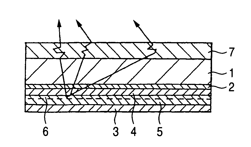
Organic electroluminescence cell, planar light source and display device
a technology of electroluminescence cell and light source, applied in the direction of luminescence screen, discharge tube, instruments, etc., can solve the problems of large luminance-improving effect, guided light beam interference with each other, and destructive interference with each other
- Summary
- Abstract
- Description
- Claims
- Application Information
AI Technical Summary
Benefits of technology
Problems solved by technology
Method used
Image

Examples
example 1
[0198]The invention will be described specifically in the following Examples 1-1 to 1-6 and Comparative Examples 1-1 to 1-6 in which a light-diffusing layer (light-diffusing tackiness agent) or a lens structure is provided as the reflection / refraction angle disturbance region in the organic EL cell according to the invention.
example 1-1
[0199]A 100 nm-thick ITO film was formed from an ITO ceramic target (In2O3:SnO2=90% by weight:10% by weight) on a surface of a glass substrate by a DC sputtering method to thereby form a transparent electrode (anode).
[0200]Then, in the condition that a photo resist was used, ITO was etched to form a pattern having a light-emitting area of 15 mm×15 mm. After ultrasonic Cleaning, ozone cleaning was performed by using a low-pressure ultraviolet lamp.
[0201]Then, organic layers were formed successively on the ITO surface by a vacuum vapor deposition method. First, CuPc represented by the formula (3) was deposited at a vapor deposition rate of 0.3 nm / s to form a 15 nm-thick hole injection layer. Next, α-NPD represented by the formula (4) was deposited at a vapor deposition rate of 0.3 nm / s to form a 40 nm-thick hole transport layer. Finally, Alq represented by the formula (5) was deposited at a vapor deposition rate of 0.3 nm / s to form a 140 nm-thick electron transport light-emitting laye...
example 1-2
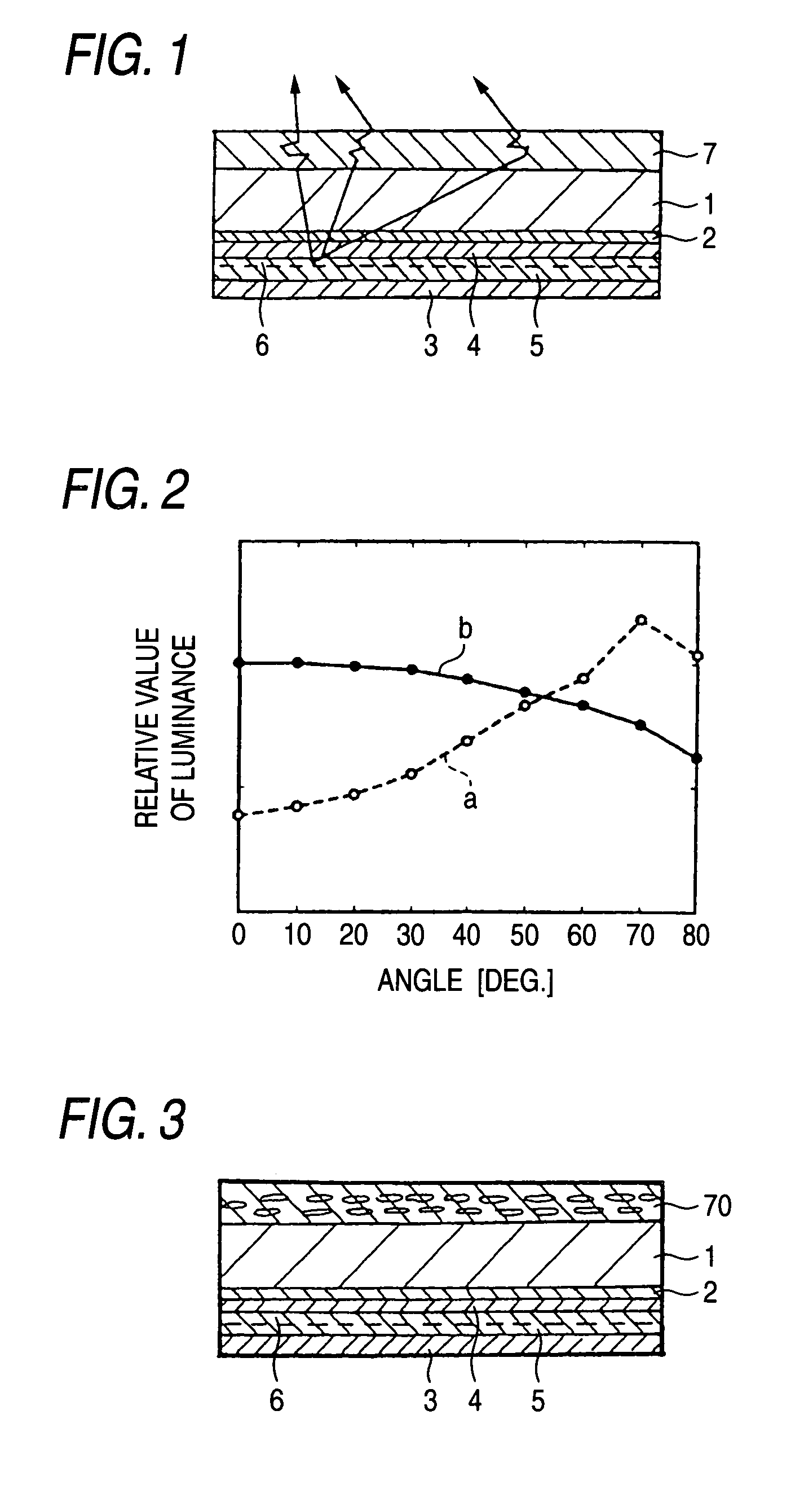
[0214]An organic EL cell as a basic configuration and an organic EL cell including a light-diffusing layer added to the basic configuration were produced in the same manner as in Example 1-1 except that a 120 nm-thick layer of Alq represented by the formula (5) was formed as the electron transport light-emitting layer.
[0215]Before and after the formation of the light-diffusing layer, a voltage of 13.1 V was applied to the organic EL cell so that a current with a current density of 10.5 mA / cm2 flew in the cell to generate luminescence in the same manner. In this condition, the organic EL cell was evaluated in the same manner as in Example 1-1. Results of the evaluation were shown in Table 1-2. Incidentally, the luminance distribution in the θ direction before the formation of the light-diffusing layer satisfied the relation given by the expression (1) of the invention, and the value of 120 nm as the thickness of the Alg layer also satisfied the relation given by the expression (2) of...
PUM
| Property | Measurement | Unit |
|---|---|---|
| Temperature | aaaaa | aaaaa |
| Angle | aaaaa | aaaaa |
| Angle | aaaaa | aaaaa |
Abstract
Description
Claims
Application Information