
System, method and apparatus for improved electrical-to-optical transmitters disposed within printed circuit boards

a technology of printed circuit boards and transmitters, applied in the field of optoelectronic systems, can solve the problems of difficult realization of effective heat dissipation, and achieve the effect of simple and reliable fabrication process

Inactive Publication Date: 2006-09-26
BOARD OF RGT THE UNIV OF TEXAS SYST
View PDF15 Cites 35 Cited by
  • Summary
  • Abstract
  • Description
  • Claims
  • Application Information

AI Technical Summary

Benefits of technology

"The present invention provides an improved heat sink for electrical-to-optical transmitters in printed circuit boards. The heat sink is embedded within the printed circuit board and is thermally coupled to the bottom surface of the transmitter. The heat sink can be fabricated using standard electrical copper plating processes, reducing manufacturing costs. The invention also provides an improved method to fabricate the reflective element and channel waveguide structure, making them easier and faster to manufacture. Overall, the invention improves heat dissipation and provides better performance for electrical-to-optical transmitters in printed circuit boards."

Problems solved by technology

In spite of the importance of dissipating heat, effective heat dissipation is very difficult to realize, especially in fully embedded board level optical interconnects due to the fact that all optical components are buried between thermally insulated materials, such as interlayer dielectric material.

Method used


Image

  • System, method and apparatus for improved electrical-to-optical transmitters disposed within printed circuit boards
  • System, method and apparatus for improved electrical-to-optical transmitters disposed within printed circuit boards
  • System, method and apparatus for improved electrical-to-optical transmitters disposed within printed circuit boards

Examples


Embodiment Construction

[0059]While the making and using of various embodiments of the present invention are discussed in detail below, it should be appreciated that the present invention provides many applicable inventive concepts that can be embodied in a wide variety of specific contexts. The specific embodiments discussed herein are merely illustrative of specific ways to make and use the invention and do not delimit the scope of the invention.

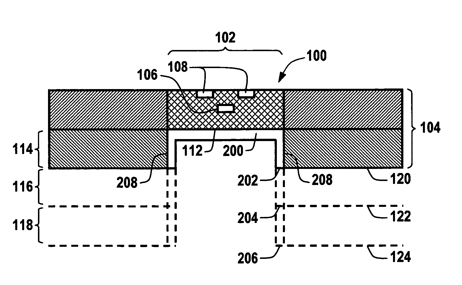
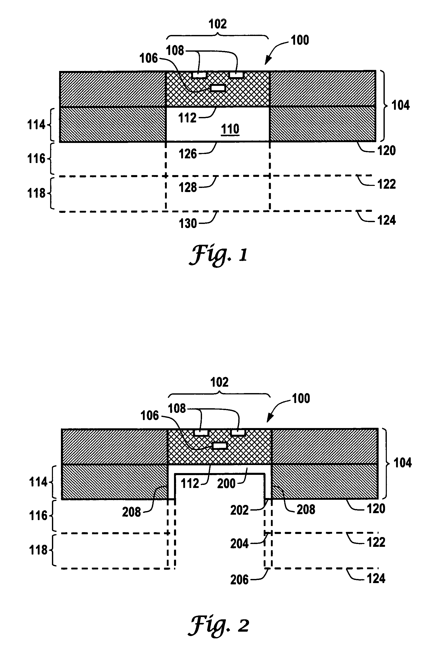
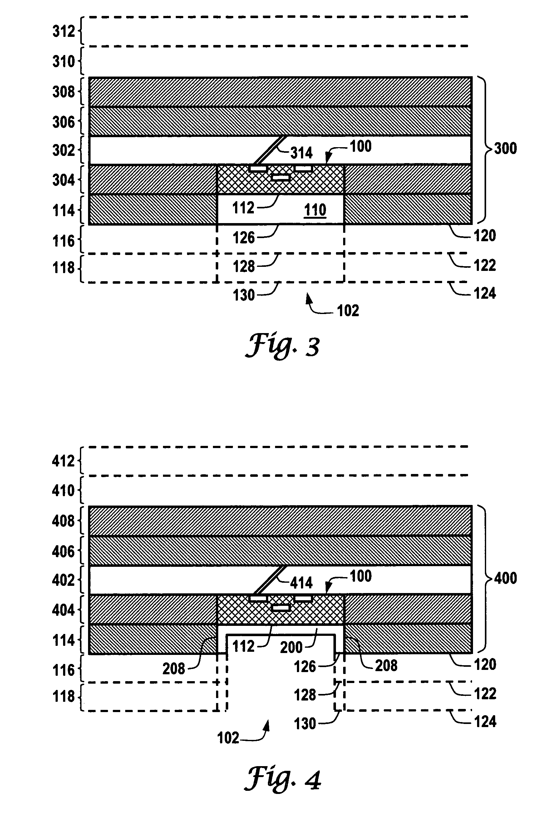
[0060]The present invention uses inventive heat dissipation and fabrication techniques to improve electrical-to-optical transmitters disposed within a printed circuit board. First, the present invention provides an effective heat sink embedded within the electro-optical hybrid printed circuit board using a simple and reliable fabrication process that does not require additional steps. Second, the present invention provides an improved method to fabricate the reflective element disposed within the channel waveguide structure. Third, the present invention provides ...


PUM


Abstract

The present invention provides a system, method and apparatus for improved electrical-to-optical transmitters (100) disposed within printed circuit boards (104). The heat sink (110, 200) is a thermal conductive material disposed within a cavity (102) of the printed circuit board (104) and is thermally coupled to a bottom surface (112) of the electrical-to-optical transmitter (100). A portion of the thermal conductive material extends approximately to an outer surface (120, 122 or 124) of a layer (114, 116 or 118) of the printed circuit board (104). The printed circuit board may comprise a planarized signal communications system or an optoelectronic signal communications system. In addition, the present invention provides a method for fabricating the heat sink wherein the electrical-to-optical transmitter disposed within a cavity of the printed circuit board is fabricated. New methods for flexible waveguides and micro-mirror couplers are also provided.

Description

PRIORITY CLAIM AND U.S. GOVERNMENT GRANTS[0001]This patent application is a U.S. non-provisional patent application of U.S. provisional patent application Ser. No. 60 / 485,496 filed on Jul. 7, 2003. This work was sponsored by United States Government grants from DARPA.FIELD OF THE INVENTION[0002]The present invention relates generally to the field of optoelectronic systems, and in particular, to a system, method and apparatus for improved electrical-to-optical transmitters disposed within printed circuit boards.BACKGROUND OF THE INVENTION[0003]Printed circuit boards (“PCBs”), multi-chip modules (“MCMs”), and similar structures having multiple integrated circuits mounted upon their surfaces are used extensively in modem electronic devices and systems. PCBs typically contain multiple conductive and dielectric layers interposed upon each other, and interlayer conductive paths (referred to as vias), which may extend from an integrated circuit mounted on a surface of the PCB to one or mor...

Claims


Application Information

Patent Timeline
Patent Type & Authority Patents(United States)
IPC IPC(8): H01L23/24H01S3/04G02B6/42G02B6/43H01L23/15H05K1/02
CPCH05K1/0274G02B6/4214H05K1/0203G02B6/43
Inventor CHEN, RAY T.CHOL, CHULCHAE
Owner BOARD OF RGT THE UNIV OF TEXAS SYST
Learn More