Level shifter for detecting grounded power-supply and level shifting method

a level shifter and power supply technology, applied in logic circuits, logic circuit coupling/interface arrangements, pulse techniques, etc., can solve the problems of additional static current consumption, large static consumption, and large static consumption

Active Publication Date: 2006-09-26
SAMSUNG ELECTRONICS CO LTD
View PDF11 Cites 44 Cited by
  • Summary
  • Abstract
  • Description
  • Claims
  • Application Information

AI Technical Summary

Benefits of technology

[0030]According to the present invention, there is provided a level shifter and associated level shifting method, which detect whether a power voltage of a low voltage stage is at the ground level and prevent an indefinite logic state of the level shifter.

Problems solved by technology

These conventional circuits commonly occupy a large area and induce additional static current consumption.
However, the pull-up / pull-down circuit 140 realized by the integrated circuit may consume large static current and requires separate control signals (PDB, PD of FIG. 1) for controlling the transistors M13′ and M14′.
When the pull-up / pull-down circuit integrated by an integrated circuit of diode-connected transistors or resistors occupies a large area and induces additional static current consumption.

Method used


Image

  • Level shifter for detecting grounded power-supply and level shifting method
  • Level shifter for detecting grounded power-supply and level shifting method
  • Level shifter for detecting grounded power-supply and level shifting method

Examples


embodiment 1

[0056]FIG. 3 is a circuit diagram of a low-to-high voltage level shifter of the FIG. 2 according to a first exemplary embodiment of the present invention.

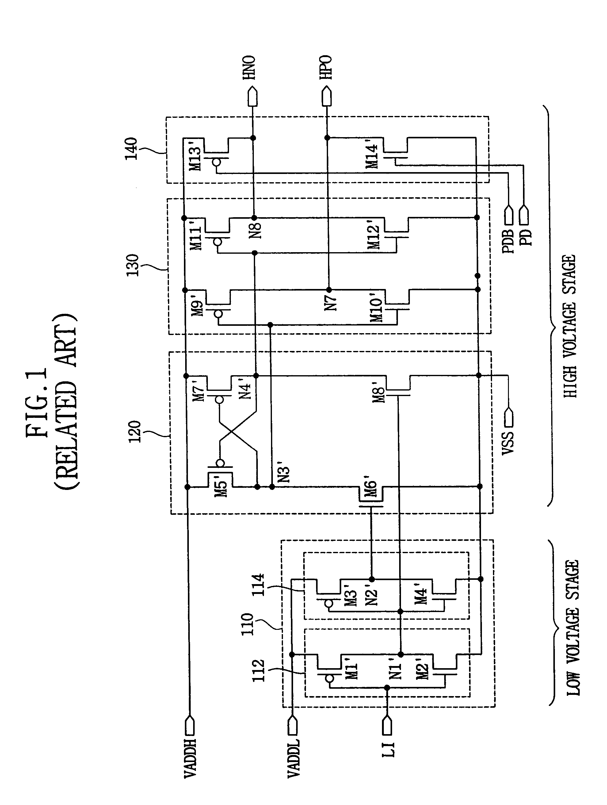
[0057]Referring to FIG. 3, an input buffer 210 has a first inverter 212 and a second inverter 214. The first inverter 212 has a PMOS transistor M1 and an NMOS transistor M2. The second inverter 214 has a PMOS transistor M3 and an NMOS transistor M4.

[0058]The input buffer 210 is activated by a first power voltage VADDL having a low-voltage level. The input buffer 210 receives a small range input signal LI via the first inverter 212, outputs a first small range signal 213 having the same phase with respect to the input signal LI via a node N2 and outputs a second small range signal 215 having a reversed phase with respect to the input signal LI via a node N1.

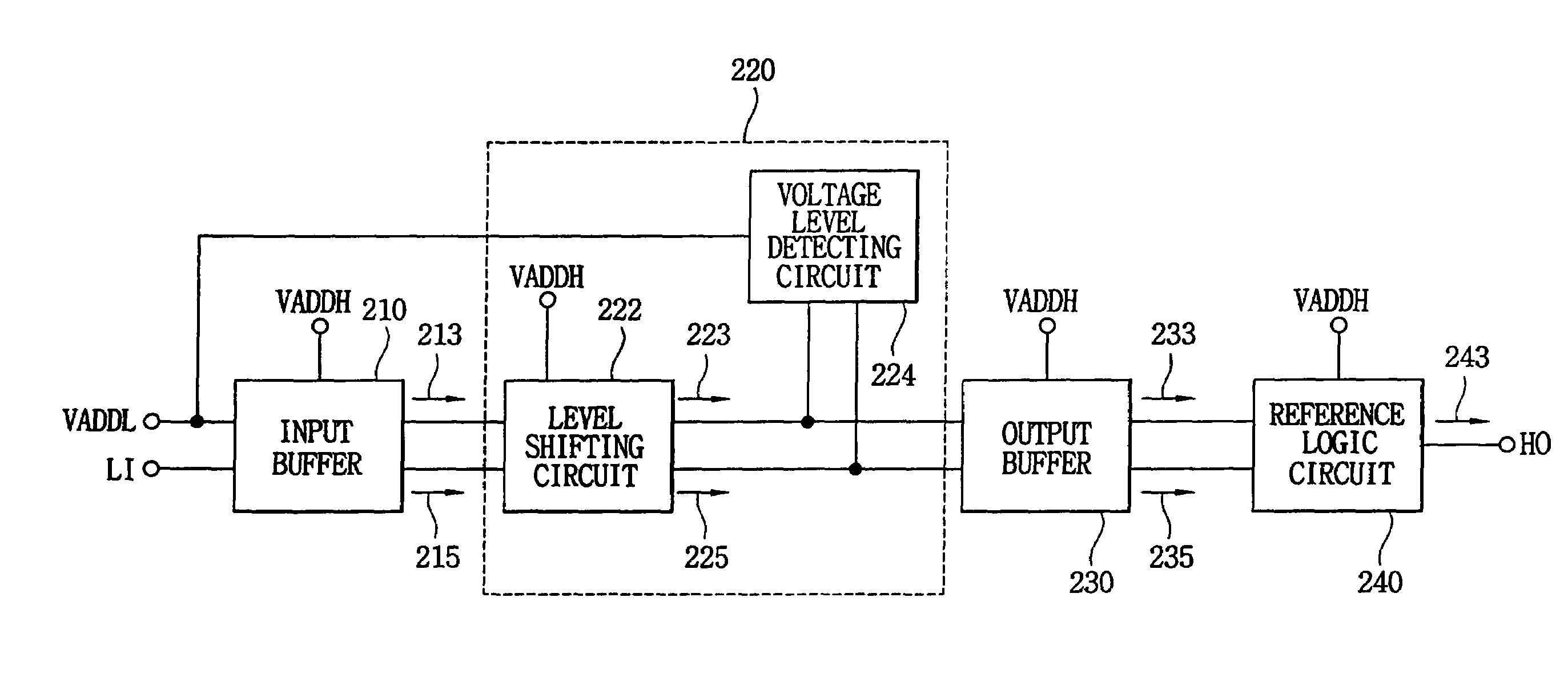
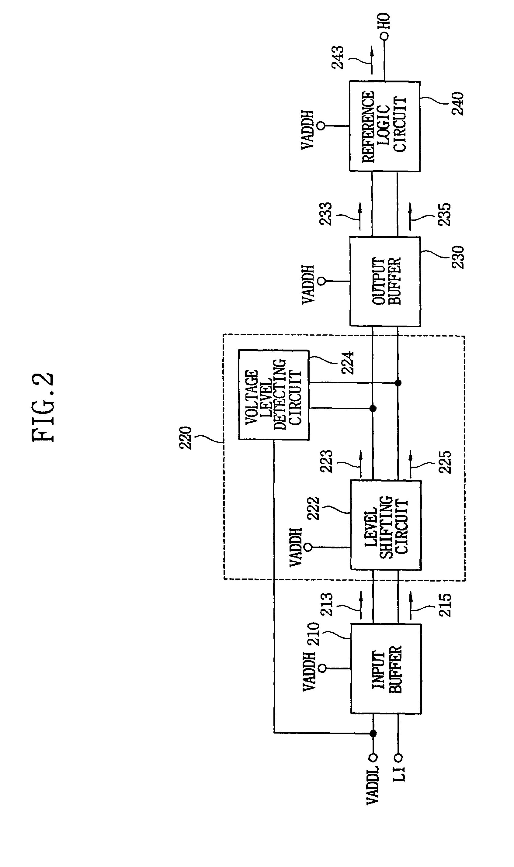
[0059]A voltage level shifting circuit 220 has a level shifting circuit 222 and a voltage level detecting circuit 224.

[0060]The level shifting circuit 222 is activated by a secon...

embodiment 2

[0115]FIG. 5 is a circuit diagram of a low-to-high voltage level shifter of FIG. 2 according to a second exemplary embodiment of the present invention.

[0116]Referring to FIG. 5, the low-to-high level shifter according to the second exemplary embodiment of the present invention has a reference logic circuit 240b that has NAND GATEs instead of the NOR GATEs. That is, the reference logic circuit 240b is implemented by using two NAND GATEs instead of two NOR GATEs. When the first power voltage VADDL is below the given voltage level, the nodes N7 and N8 have the high-voltage logic level ‘LOW’ and the output signal HO has the high-voltage logic level ‘HIGH’.

[0117]Hereinafter, an input buffer 210, a level shifting circuit 222, a voltage level detecting circuit 224 and an output buffer 230 of the low-to-high level shifter according to the second exemplary embodiment of the present invention are the same as those of the low-to-high level shifter according to the first exemplary embodiment of...


PUM


Abstract

A level shifter includes an input buffer, a level shifting circuit, a voltage level detecting circuit, an output buffer and a reference logic circuit. The input buffer buffers a small range input signal to output a small range signal. The level shifting circuit transforms the small range signal into a first wide range signal. The voltage level detecting circuit detects whether a power voltage of a low voltage stage is at the ground level, and prevents an indefinite logic state of the level shifter. The output buffer buffers the first wide range signal to output a second wide range signal. The reference logic circuit generates a wide range signal having a predetermined logic status when the power voltage is at the ground level. Thus, a leakage current of the level shifter is reduced.

Description

CROSS-REFERENCE TO RELATED APPLICATIONS[0001]This application relies for priority upon Korean Patent Application No. 2003-53533 filed on Aug. 1, 2003, the contents of which are herein incorporated by reference in its entirety.BACKGROUND OF THE INVENTION[0002]1. Field of the Invention[0003]The present invention relates to a voltage level shifter and a level shifting method for shifting a small range signal to a wide range signal.[0004]2. Description of the Related Art[0005]Generally, laptop computers and portable devices require low power consumption, and widely adopt a multi-power architecture which implements a small range voltage and a wide range voltage are used. Typically, such multi-power architectures require level-shifting circuits to provide voltage and power driving interfaces between circuits operating at different power voltage levels. Such level shifting circuits commonly include an input buffer receiving an input signal driven at a first power supply voltage level, a le...

Claims


Application Information

Patent Timeline
Patent Type & Authority Patents(United States)
IPC IPC(8): H03K19/0175H03K19/094H03K3/356
CPCH03K3/356113H03K3/356008H03K19/0175
Inventor LEE, JONG-HWA
Owner SAMSUNG ELECTRONICS CO LTD
Why Eureka
Try Eureka