Lateral power MOSFET for high switching speeds

a lateral power mosfet and high switching speed technology, applied in the field of semiconductor devices, can solve the problems of high gate-to-drain capacitance, degrade the high-speed switching performance of the transistor, and cause high gate-to-drain capacitan

Inactive Publication Date: 2006-10-03
POWER INTEGRATIONS INC
View PDF39 Cites 66 Cited by
  • Summary
  • Abstract
  • Description
  • Claims
  • Application Information

AI Technical Summary

Problems solved by technology

One drawback associated with the lateral power transistor structure taught by the '277 patent is high gate-to-drain capacitance due to the proximate location of the gate and drain electrodes.
But in the case where the device is designed for a much lower voltage, the closer spacing between the drain electrode and the gate electrode results in high gate-to-drain capacitance.
This large capacitance degrades the high-speed switching performance of the transistor.
High gate-to-drain capacitance is especially problematic because it is amplified by the gain of the transistor.

Method used


Image

  • Lateral power MOSFET for high switching speeds
  • Lateral power MOSFET for high switching speeds
  • Lateral power MOSFET for high switching speeds

Examples


Embodiment Construction

[0011]A high-voltage lateral power MOSFET with reduced gate-to-drain capacitance for high switching speeds is described. In the following description, numerous specific details are set forth, such as material types, dimensions, structural features, etc., in order to provide a thorough understanding of the present invention. Practitioners having ordinary skill in the semiconductor arts will understand that the invention may be practiced without many of these details. In other instances, well-known elements, techniques, and processing steps have not been described in detail to avoid obscuring the invention.

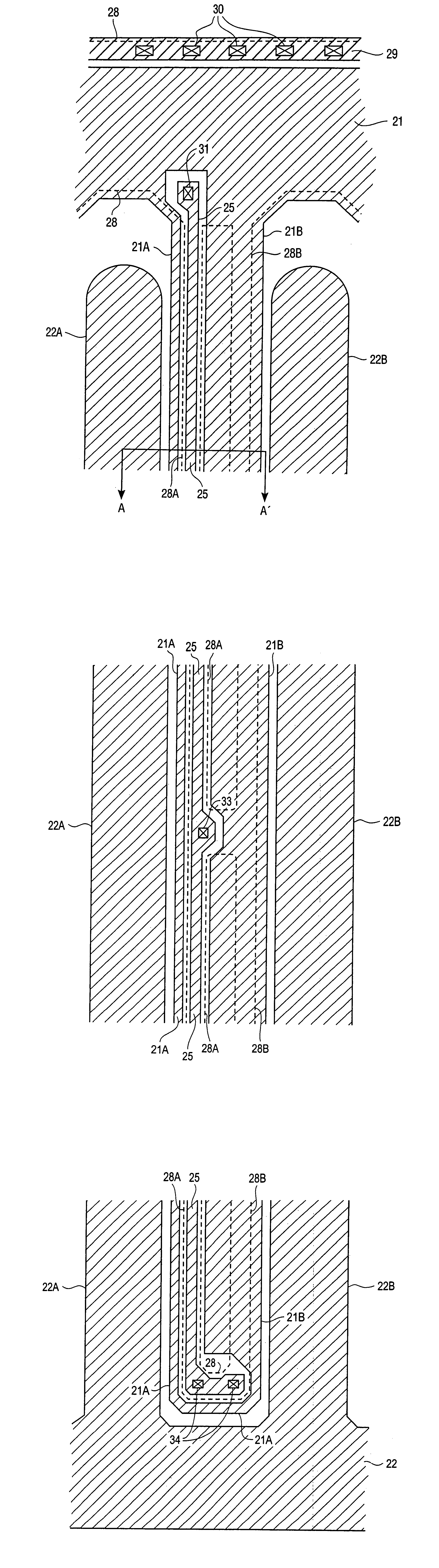
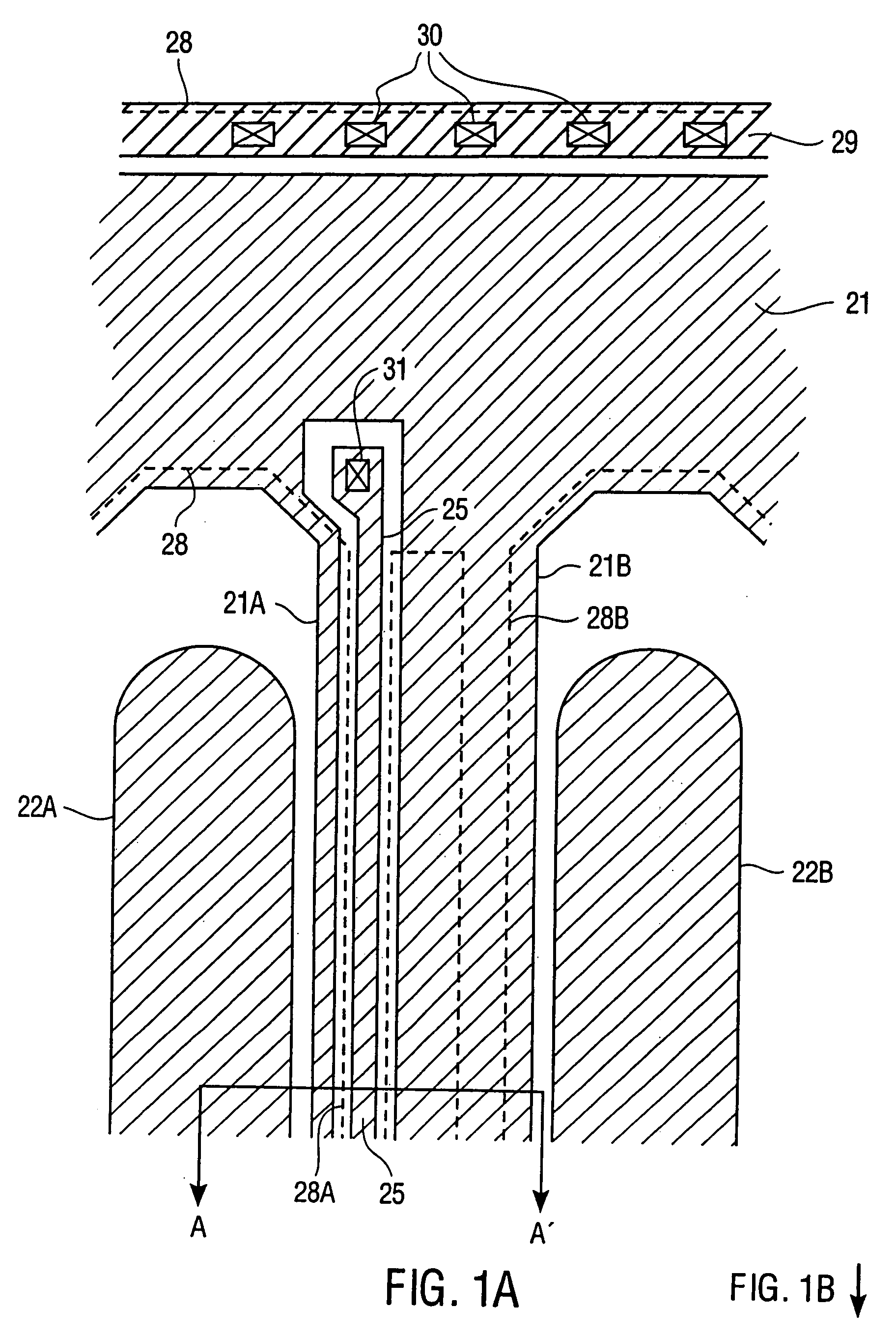
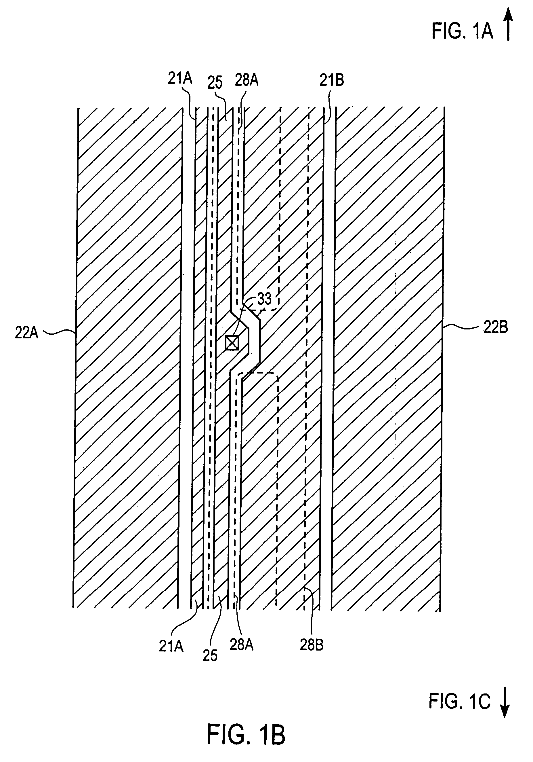
[0012]The field effect transistor of the present invention includes a metal gate electrode coupled with an insulated gate disposed over a channel region that separates elongated source and drain regions of the power MOSFET. In one embodiment the gate comprises polysilicon, and the gate electrode is coupled to the polysilicon gate using metal contacts (also known as vias) that are lo...


PUM


Abstract

A lateral power metal-oxide-semiconductor field effect transistor (MOSFET) having a gate structure in which the insulated gate is coupled to the gate electrode through contacts at a plurality of locations. The source electrode includes first and second segments. The first segment is interposed between the drain electrode and the gate electrode and acts as a field plate.

Description

FIELD OF THE INVENTION[0001]The present invention relates to semiconductor devices fabricated in a silicon substrate. More specifically, the present invention relates to a high voltage field effect transistor with an improved gate design.BACKGROUND OF THE INVENTION[0002]A common type of integrated circuit device is a metal-oxide-semiconductor field effect transistor (MOSFET). A MOSFET is a field effect device that includes a source region, a drain region, a channel region extending between the source and drain regions, and a gate provided over the channel region. The gate includes a conductive gate structure disposed over and separated from the channel region with a thin oxide layer.[0003]Lateral field-effect transistors are widely used for high voltage circuit applications, e.g., greater than 200 volts. Examples of traditional lateral MOSFET device structures for power applications include U.S. Pat. Nos. 5,869,875, 5,821,144, 5,760,440, and 4,748,936. Each of these devices has a so...

Claims


Application Information

Patent Timeline
Patent Type & Authority Patents(United States)
IPC IPC(8): H01L29/76H01L29/40H01L29/417H01L29/423H01L29/78
CPCH01L29/402H01L29/41758H01L29/41775H01L29/42372H01L29/4238H01L29/7835H01L29/41725H01L29/42368
Inventor DISNEY, DONALD RAYGRABOWSKI, WAYNE BRYAN
Owner POWER INTEGRATIONS INC
Why Eureka
Try Eureka