Production method of a vertical type MOSFET

Inactive Publication Date: 2000-01-18
DENSO CORP
View PDF55 Cites 60 Cited by
  • Summary
  • Abstract
  • Description
  • Claims
  • Application Information

AI Technical Summary

Benefits of technology

It is an object of the present invention to provide a vertical

Problems solved by technology

However, the R-MOS device has drawbacks in that the yield and the reliability are low.
The cause is that the trench groove 50 is formed by the reactive ion etching method, and therefore the flatness of the sidewall surface of the inner wall 51 is bad and produces many defects, and the film quality of the gate oxide film 8, which is formed by oxidizing the surface thereof, is bad.
Insulation inferiority of the gate oxide film, a decrease in the mobility due to the defect of the interface of the channel por

Method used


Image

  • Production method of a vertical type MOSFET
  • Production method of a vertical type MOSFET
  • Production method of a vertical type MOSFET

Examples


first embodiment

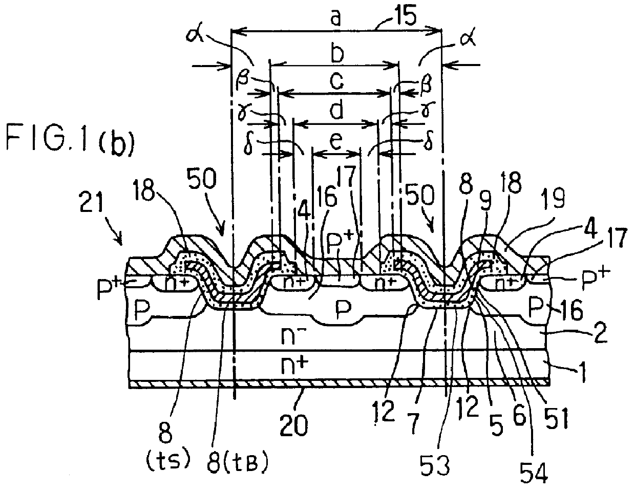
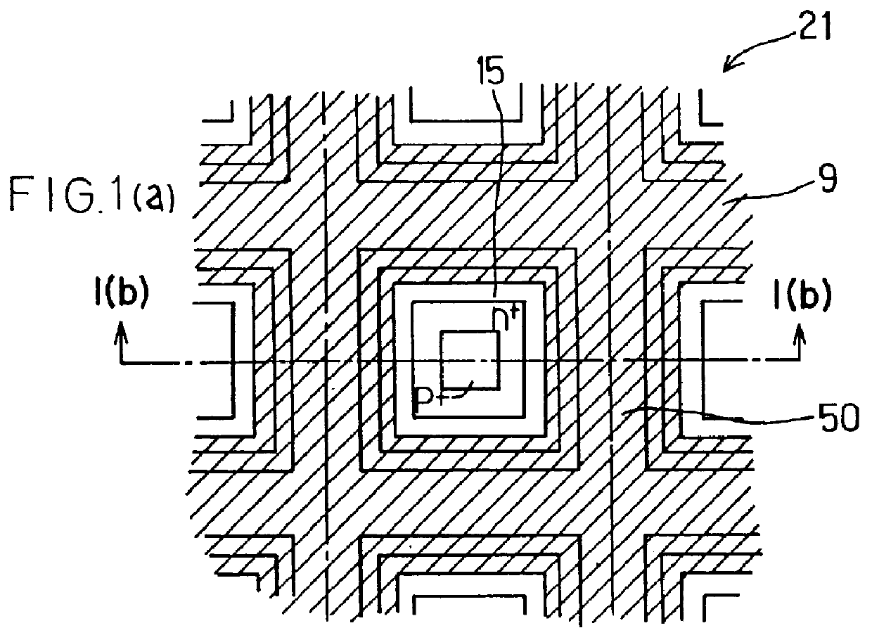
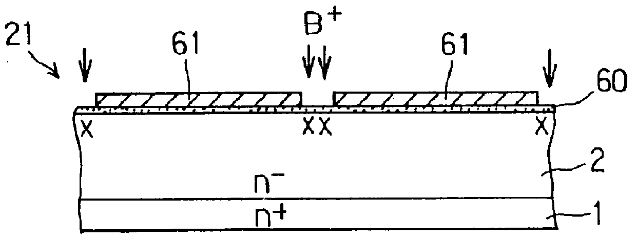
FIG. 1(a) is a plane view of a vertical power MOSFET comprising rectangular unit cells according to the present invention, and FIG. 1(b) is a cross-sectional view taken along A--A in FIG. 1(a). FIG. 2 to FIG. 13 are also cross-sectional views of a wafer as each step progresses in the production of the vertical type power MOSFET, which corresponds to FIG. 1(b). Incidentally, FIG. 2 is a cross-sectional view of the wafer subjected to boron ion implantation for the formation of the central portion of a p-type base layer, FIG. 3 is a cross-sectional view of the wafer subjected to patterning of a silicon nitride film at an interval of a unit cell size a for the LOCOS oxidation, FIG. 4 is a cross-sectional view of the wafer subjected to wet etching using a window of the silicon nitride film, FIG. 5 is a cross-sectional view of the wafer in which a LOCOS oxide film is formed, FIG. 6 is a cross-sectional view of the wafer subjected to boron ion implantation for the formation of the p-type b...

second embodiment

For example, in the second embodiment shown in FIG. 22, a source electrode 19 is allowed to make ohmic contact with an n.sup.+ -type source layer 4 and a p.sup.+ -type base contact layer 17 through a groove 52, and especially there is given a structure in which the source electrode 19 makes ohmic contact with the side face of the n.sup.+ -type source layer 4. In order to fabricate this structure, in the production steps shown in FIG. 2 to FIG. 13, the n.sup.+ -source layer 4 is diffused and formed on the whole face of the upper face of the p-type base layer 16 to constitute the gate structure, and further when the contact hole is opened through the interlayer insulation film 18, a groove 52 may be formed penetrating through the interlayer insulation film 18 and the n.sup.+ -type source layer 4 to arrive at the p.sup.+ -type base contact layer 17. Incidentally, setting can be made variously such that the p.sup.+ -type base contact layer 17 is formed before the formation of the n.sup....

third embodiment

In the third embodiment, in FIG. 2, the wafer 21 is selected to have the index of plane of its main surface which is (1 1 1) or those near it. Thus the surface of the n.sup.- -type epitaxial layer 2 corresponding to the bottom face of the LOCOS oxide film 65 formed on the wafer 21 in the step shown in FIG. 5, that is the bottom face 53 of the U-groove 50 is parallel to the main surface, so that its index of plane is also (1 1 1).

In addition, in FIG. 1(a), owing to the optimization of the surface directions of the sides of the rectangular unit cell 15 with respect to the surface direction of the main surface of the wafer 21, and the optimization of the inclination angle of the side face 54 of the U-groove 50 by condition setting in the LOCOS oxidation step shown in FIG. 5, the index of plane of the side face 54 of the U-groove 50 is set to be an index near (1 0 0) in which the interface state density is less.

Thus in the step for forming the gate oxide film 8 shown in FIG. 10, dependi...


PUM


Abstract

A vertical type power MOSFET remarkably reduces its ON-resistance per area. A substantial groove formation in which a gate structure is constituted is performed beforehand utilizing the LOCOS method before the formation of a p-type base layer and an n+-type source layer. The p-type base layer and the n+-type source layer are then formed by double diffusion in a manner of self-alignment with respect to a LOCOS oxide film, simultaneously with which channels are set at sidewall portions of the LOCOS oxide film. Thereafter the LOCOS oxide film is removed to provide a U-groove so as to constitute the gate structure. Namely, the channels are set by the double diffusion of the manner of self-alignment with respect to the LOCOS oxide film, so that the channels, which are set at the sidewall portions at both sides of the groove, provide a structure of exact bilateral symmetry, there is no positional deviation of the U-groove with respect to the base layer end, and the length of the bottom face of the U-groove can be made minimally short. Therefore, the unit cell size is greatly reduced, and the ON-resistance per area is greatly decreased.

Description

1. Technical FieldThe present invention relates to a vertical type MOSFET (Metal Oxide Semiconductor Field Effect Transistor) to be used as a semiconductor device for electric power, which is preferable in the case of adoption as MOSIC and the like in which an elemental article thereof or the semiconductor device for electric power is incorporated.2. Background ArtThe vertical type power MOSFET has many features such that it has excellent frequency characteristics, has a fast switching velocity, can be driven at low electric power and the like, so that it has recently been used in many industrial fields. For example, in "Nikkei Electronics" published by Nikkei-McGraw-Hill, Inc. on May 19, 1986, pp. 165-188, it is described that the focus of development of the power MOSFET is in migrating to low voltage resistant articles and high voltage resistant articles. Further, it is described in this literature that the ON-resistance of a power MOSFET chip having a voltage resistance not more ...

Claims


Application Information

Patent Timeline
IPC IPC(8): H01L29/40H01L21/336H01L29/06H01L29/423H01L21/02H01L29/78H01L29/02H01L29/66H01L29/04
CPCH01L29/045H01L29/0696H01L29/7813H01L29/4236
Inventor TOKURA, NORIHITOTAKAHASHI, SHIGEKIYAMAMOTO, TSUYOSHIKATAOKA, MITSUHIRO
Owner DENSO CORP
Why Eureka
Try Eureka