Semiconductor device

a technology of semiconductor devices and semiconductors, applied in semiconductor devices, diodes, electrical devices, etc., can solve the problems of more likely deterioration, and achieve the effect of effective prevention of deterioration

Inactive Publication Date: 2012-03-01
RENESAS ELECTRONICS CORP
View PDF6 Cites 62 Cited by
  • Summary
  • Abstract
  • Description
  • Claims
  • Application Information

AI Technical Summary

Benefits of technology

[0014]The bidirectional Zener diode has the withstand voltage with its gate side negatively biased and that with the gate side positively biased, different from each other. The bidirectional Zener diode has (1) a source side first conductivity type region, (2) a gate side first conductivity type region having substantially the same impurity concentration as that of the source side first conductivity type region and formed in a part nearer to the gate in a circuit, and (3) a second conductivity type region coupled in series between the source side first conductivity type region and the gate side first conductivity type region, forming a source side PN junction between the source side first conductivity type region and itself , and forming a gate side PN junction between the gate side first conductivity type region and itself. The second conductivity type region has concentrations differ from each other in both end parts thereof, and therefore, it is possible to effectively prevent deterioration caused by ESD (Electro-Static Discharge) of the gate insulating film.

Problems solved by technology

On the other hand, in the case of a P-channel type power MOSFET, the deterioration is more likely to occur when the gate side bias is positive because a majority carrier is a hole.

Method used


Image

  • Semiconductor device
  • Semiconductor device
  • Semiconductor device

Examples


Embodiment Construction

Outline of Embodiments

[0058]First, the outline of typical embodiments of the inventions disclosed in the present application is explained.

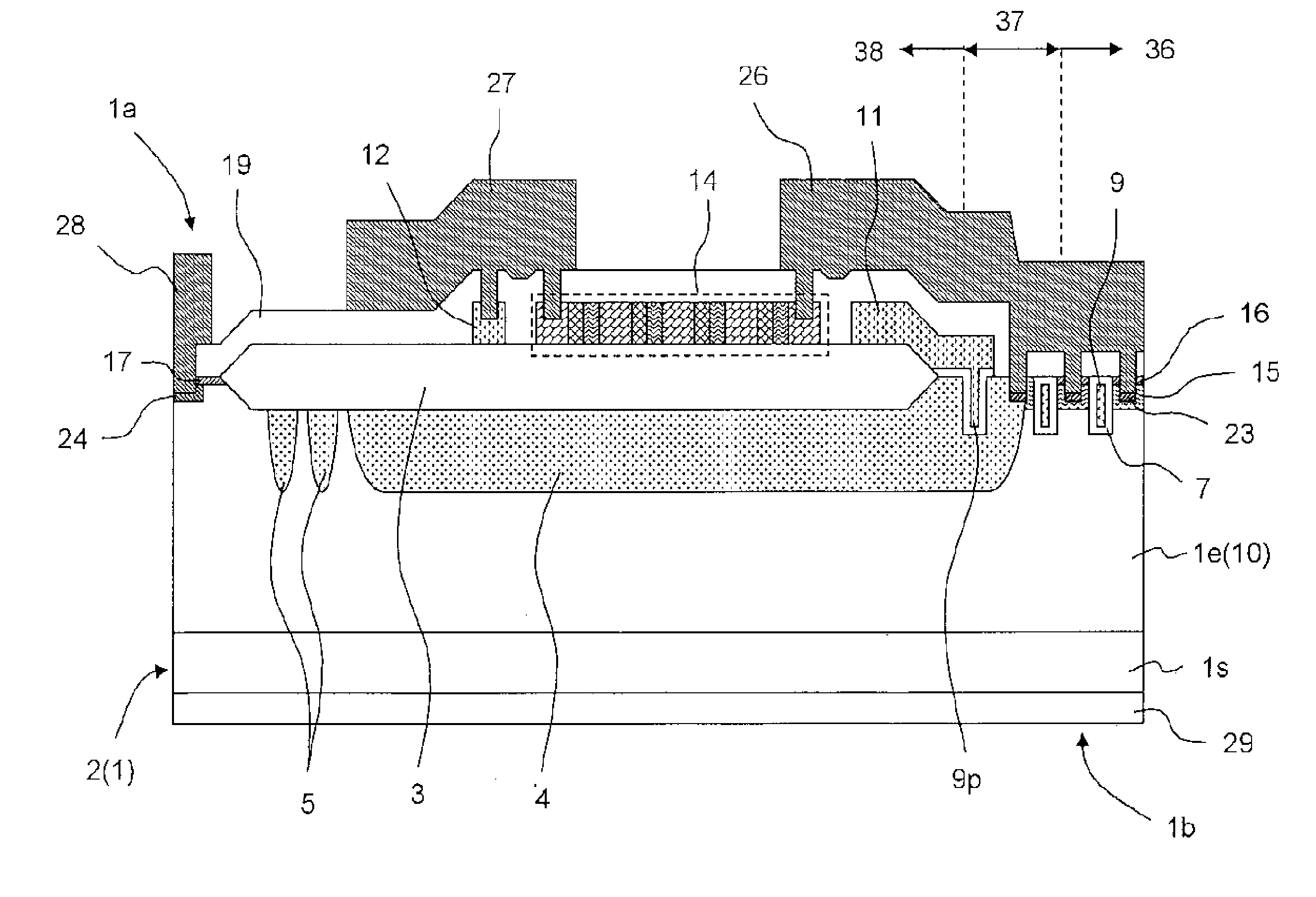
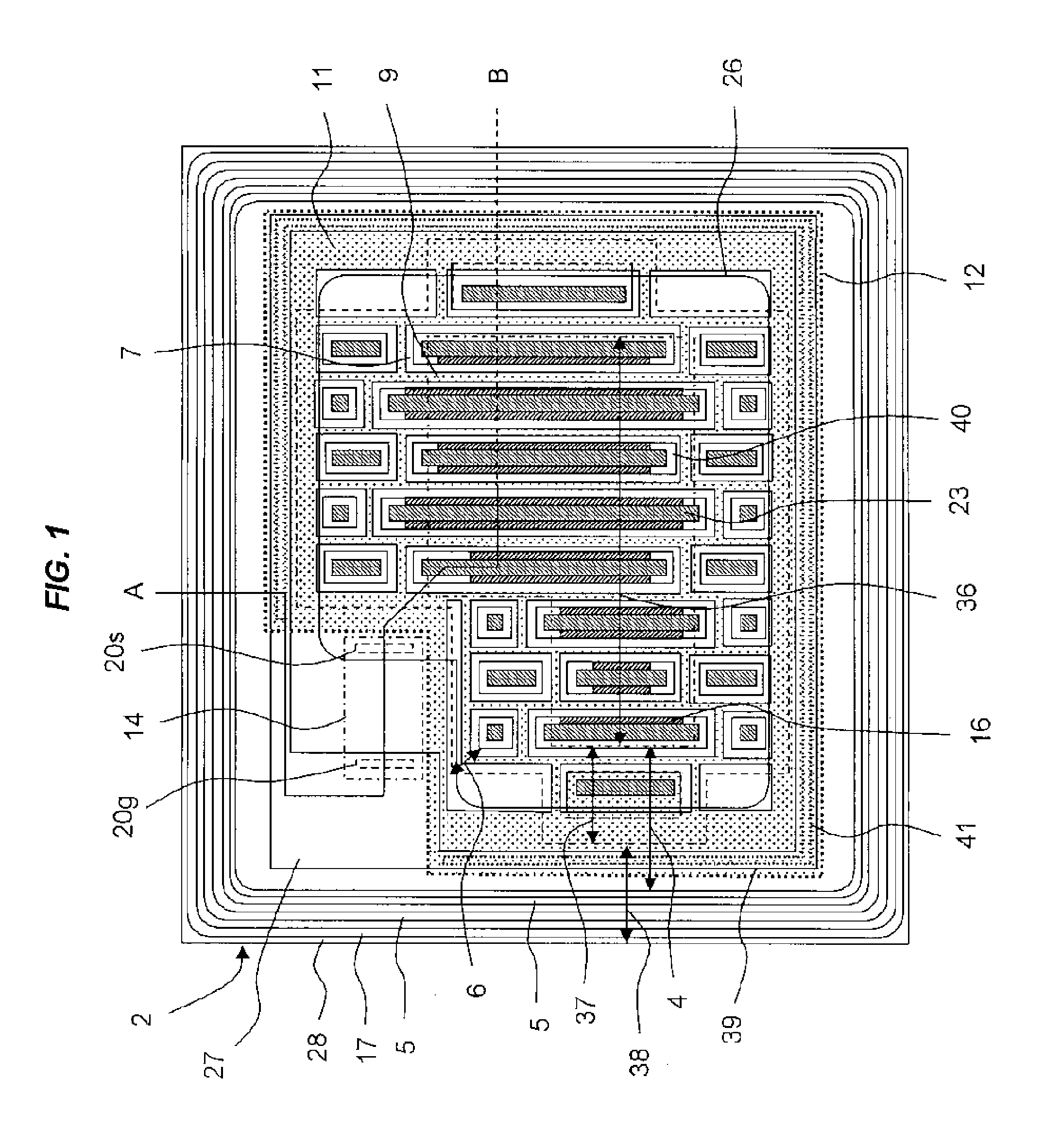
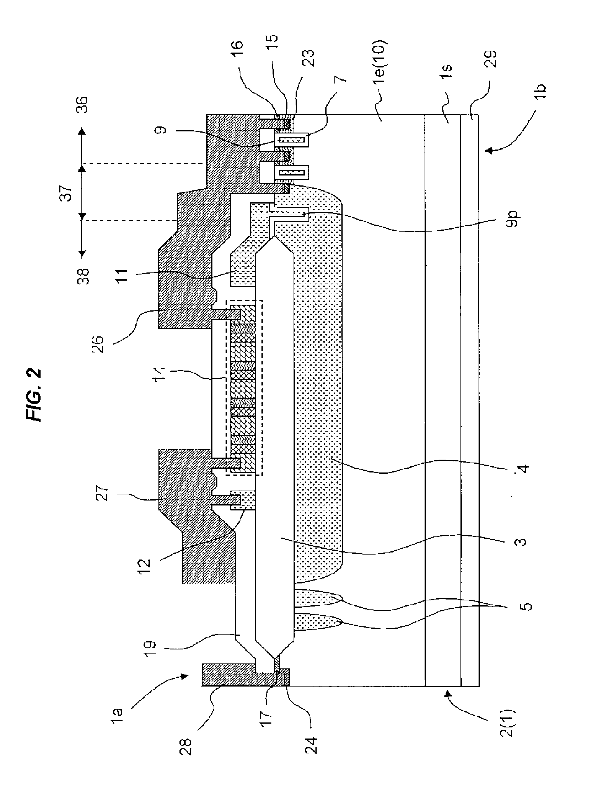
[0059]1. A semiconductor device, comprising:

[0060](a) a semiconductor chip;

[0061](b) an insulating gate power transistor formed on the semiconductor chip; and

[0062](c) a gate protection element formed in the semiconductor chip and coupled between a gate terminal and a source terminal of the insulating gate power transistor,

[0063]the gate protection element including a bidirectional Zener diode having a multistage PN junction,

[0064]wherein the bidirectional Zener diode has

[0065]the withstand voltage with its gate terminal side negatively biased and the withstand voltage with the gate terminal side positively biased, different from each other, and wherein the bidirectional Zener diode includes: (x1) a source side first conductivity type region; (x2) a gate side first conductivity type region having substantially the same impurity concentration as th...


PUM


Abstract

Accompanying the miniaturization of a gate electrode of a trench gate power MOSFET, the curvature of the bottom part of the trench increases, and thereby, electric fields concentrate on the part and deterioration of a gate oxide film (insulating film) occurs. The deterioration of the gate insulating film is more likely to occur when the gate side bias is negative in the case of an N-channel type power MOSFET and when the gate side bias is positive in the case of a P-channel type power MOSFET.
The present invention is a semiconductor device including an insulating gate power transistor etc. in a chip, wherein a gate protection element includes a bidirectional Zener diode and the bidirectional Zener diode has a plurality of P-type impurity regions (or a P-type impurity region) having different concentrations so that the withstand voltage with its gate side negatively biased and the withstand voltage with the gate side positively biased are different from each other.

Description

CROSS-REFERENCE TO RELATED APPLICATION[0001]The disclosure of Japanese Patent Application N 2010-195410 filed on Sep. 1, 2010 including the specification, drawings and abstract is incorporated herein by reference in its entirety.BACKGROUND[0002]The present invention relates to technology effective when applied to surge voltage protection technology in a semiconductor device (or semiconductor integrated circuit device).[0003]Japanese Patent Laid-Open No. 1998-65157 (Patent Document 1) discloses technology to provide an N+PN+-type Zener protection element over a field oxide film in a P-channel type power MOSFET (Metal Oxide Semiconductor Field Effect Transistor).[0004]Japanese Patent Laid-Open No. 2006-324570 (Patent Document 2) or United States Patent Application Publication No. 2009-230467 (Patent Document 3) corresponding to the former discloses technology to form a protection diode to prevent electrostatic breakdown of a gate insulating film and an embedded field plate in a polysi...

Claims


Application Information

Patent Timeline
Patent Type & Authority Applications(United States)
IPC IPC(8): H01L27/07
CPCH01L29/0619H01L29/0638H01L29/0692H01L29/0696H01L29/407H01L29/866H01L29/7397H01L29/7808H01L29/7811H01L29/7813H01L29/66734
Inventor HARUYAMA, MASAMITSUSEKI, TATSUHIROARAI, DAISUKE
Owner RENESAS ELECTRONICS CORP
Why Eureka
Try Eureka