Silicon oxycarbide and silicon carbonitride based materials for MOS devices

a technology of silicon carbonitride and silicon oxycarbide, which is applied in the direction of semiconductor devices, semiconductor/solid-state device details, electrical apparatus, etc., can solve the problems of difficult control of the etching process in order to not over-etch, degrade the device performance, and relatively thick layers, etc., to achieve lower deposition temperature, lower k values, and higher deposition rate

Active Publication Date: 2006-10-03
TAIWAN SEMICON MFG CO LTD
View PDF5 Cites 29 Cited by
  • Summary
  • Abstract
  • Description
  • Claims
  • Application Information

AI Technical Summary

Benefits of technology

[0006]The SiCO and SiCN based materials have lower k values than silicon nitride (SiN). In addition, they may be deposited at higher deposition rates and at lower deposition temperatures. By using the SiCO and SiCN based materials in the MOS device, the characteristics of the device such as the outer fringing capacitance, contact resistance, sheet resistance, threshold voltage, and leakage current are either improved or comparable to the prior art.

Problems solved by technology

The ILD layer is relatively thick, and it is hard to control the etching process in order to not over etch.
The high k value increases high parasitic capacitance, which degrades the device performance.
Additionally, the deposition rate of the silicon nitride film is low and the deposition temperature is high, which are not desirable process characteristics.

Method used


Image

  • Silicon oxycarbide and silicon carbonitride based materials for MOS devices
  • Silicon oxycarbide and silicon carbonitride based materials for MOS devices
  • Silicon oxycarbide and silicon carbonitride based materials for MOS devices

Examples


Embodiment Construction

[0015]The making and using of the presently preferred embodiments are discussed in detail below. It should be appreciated, however, that the present invention provides many applicable inventive concepts that can be embodied in a wide variety of specific contexts. The specific embodiments discussed are merely illustrative of specific ways to make and use the invention, and do not limit the scope of the invention.

[0016]The preferred embodiments of the present invention use silicon oxycarbide (SiCO) and silicon carbonitride (SiCN) based material, such as carbon-doped oxide (CDO) and nitride-doped silicon carbide (NDC) to make MOS devices. The details of making the preferred embodiments are discussed. The test results of the MOS devices are then discussed.

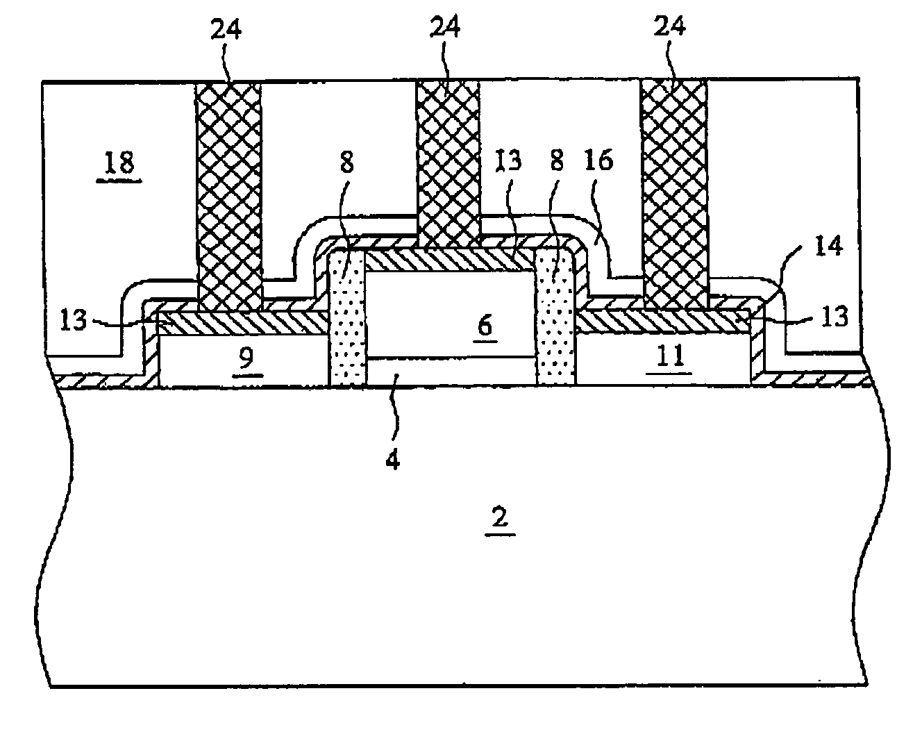
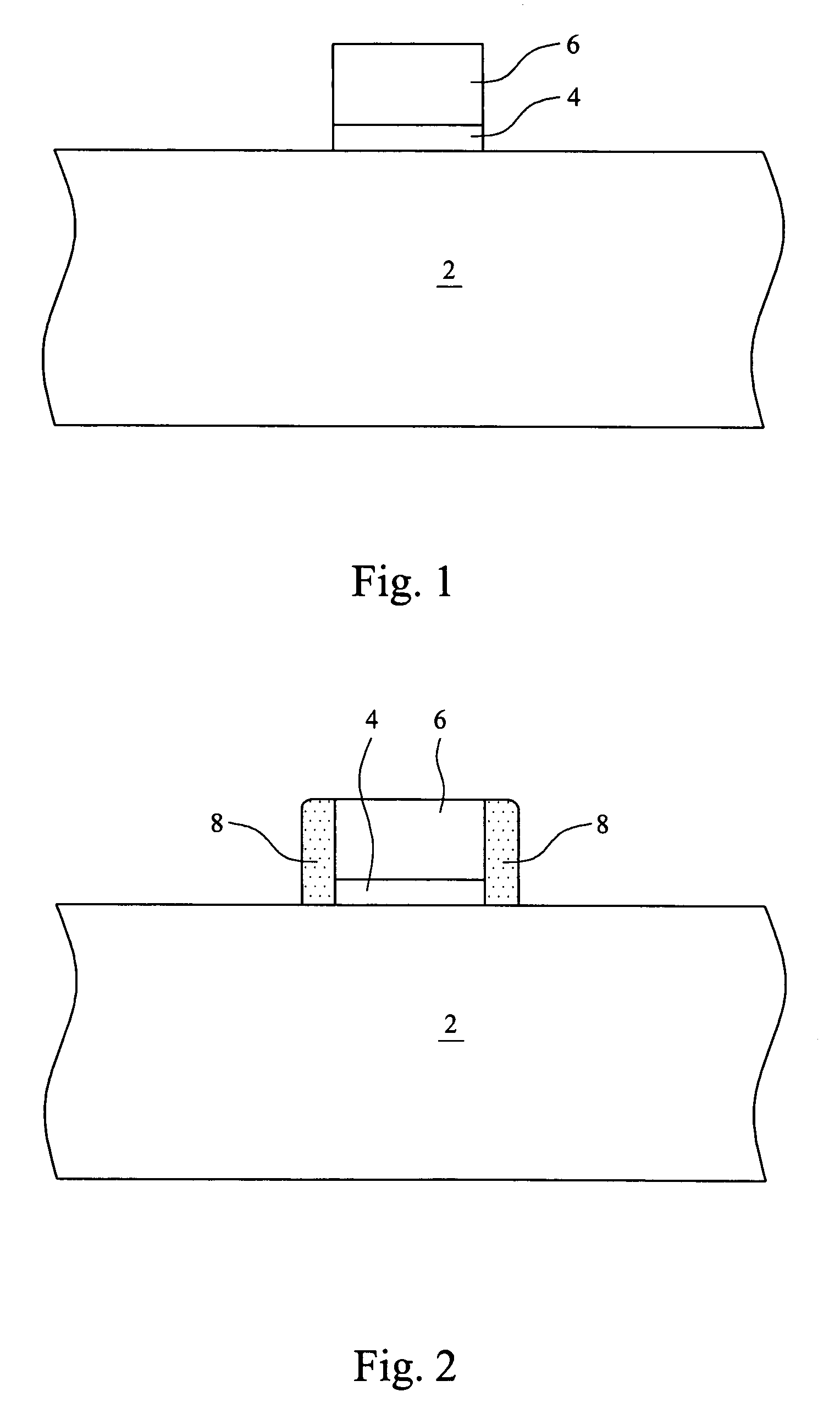
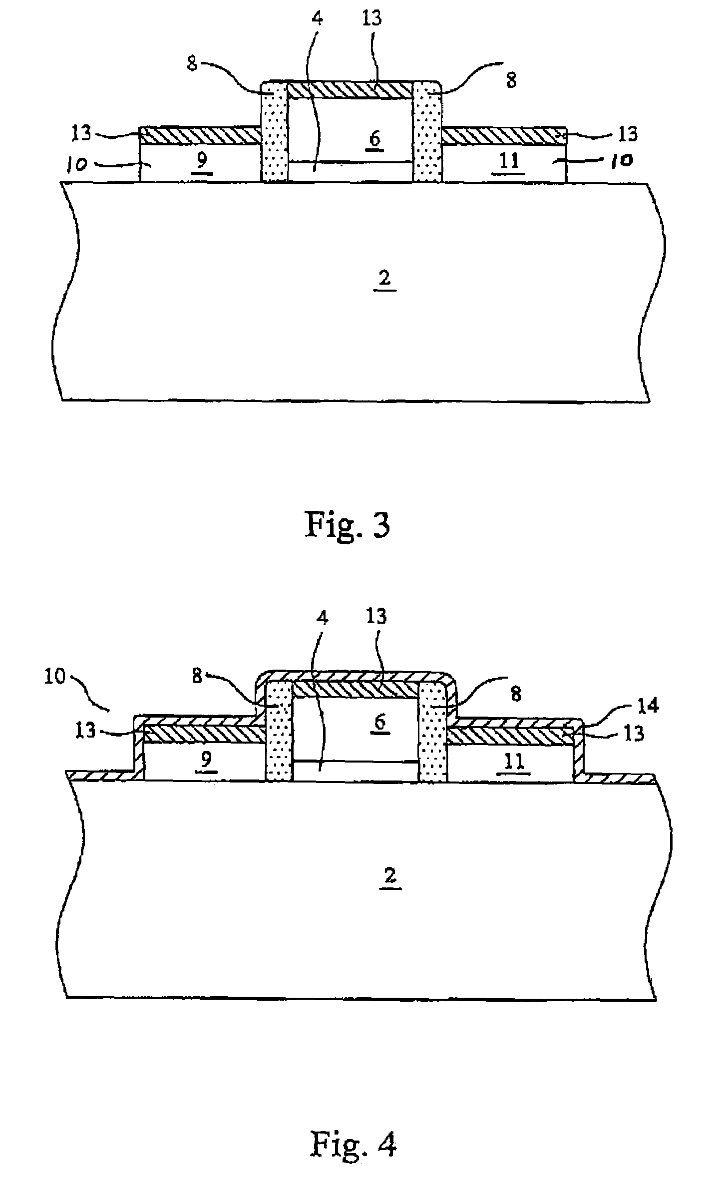
[0017]FIGS. 1 through 7 illustrate the preferred embodiments of the present invention. FIG. 1 illustrates the formation of a gate. In an illustrative embodiment, the substrate 2 is a silicon substrate. In other embodiments, silicon ger...


PUM

PropertyMeasurementUnit
dielectric constantaaaaaaaaaa
aspect ratioaaaaaaaaaa
dielectric constantaaaaaaaaaa

Abstract

In the preferred embodiment, a gate dielectric and an electrode are formed on a substrate. A pair of spacers is formed along opposite sidewalls of the gate electrode and the gate dielectric. Spacers are preferably formed of SiCO based material or SiCN based material. The source and drain are then formed. A contact etch stop (CES) layer is formed on the source / drain regions and the spacers. The CES layer is preferably formed of SiCO based material or SiCN based material. An Inter-Level Dielectric (ILD) is then formed on the CES layer.

Description

[0001]This applications claims priority to provisional patent application Ser. No. 60 / 565,630, filed Apr. 27, 2004, and entitled “Silicon Oxycarbide and Silicon Carbonitride Based Materials for MOS Devices,” which application is incorporated herein by reference.FIELD OF INVENTION[0002]This invention relates generally to semiconductor devices, and more specifically to contact etch stop layers.BACKGROUND[0003]In deep sub micron microelectronic manufacturing, silicon nitride films are widely employed as stop layers during contact etching. As is well known in the art, the inter-level dielectric (ILD) is formed to provide insulation between the MOS devices and overlying metal lines that will be formed subsequently. The contact openings are made through the ILD layer to the source, drain and gate. The ILD layer is relatively thick, and it is hard to control the etching process in order to not over etch. The contact etch stop layer is formed prior to the formation of the ILD layer. A first...

Claims


Application Information

Patent Timeline
Patent Type & Authority Patents(United States)
IPC IPC(8): H01L23/58H01L21/31H01L21/314H01L21/316H01L21/336H01L21/768H01L23/31H01L29/49
CPCH01L21/02126H01L21/02167H01L21/022H01L21/02211H01L21/02274H01L21/314H01L21/3148H01L21/31633H01L21/76832H01L21/76834H01L23/3192H01L29/4983H01L29/66628H01L2924/0002H01L21/76829H01L29/665H01L29/66636H01L2924/19041H01L2924/00
Inventor WU, ZHEN-CHENGTSAI, HUNG CHUNLIN, DA-WENCHANG, WENGCHENG, SHWANG-MINGLIANG, MONG SONG
Owner TAIWAN SEMICON MFG CO LTD
Why Eureka
Try Eureka