Micromachined probe apparatus and methods for making and using same to characterize liquid in a fluidic channel and map embedded charge in a sample on a substrate

a micromachined probe and probe apparatus technology, applied in the direction of material analysis using wave/particle radiation, instruments, nuclear engineering, etc., can solve the problems of limiting the application of micromachined probes, unable to measure local charge distributions on patterned wafers, etc., and achieve the effect of varying the capacitan

Active Publication Date: 2006-10-03
WISCONSIN ALUMNI RES FOUND +1
View PDF10 Cites 6 Cited by
  • Summary
  • Abstract
  • Description
  • Claims
  • Application Information

AI Technical Summary

Problems solved by technology

Conventional plasma damage characterization approaches [Fri97, Cis98, Fan92] are based on electrical or surface analytical techniques, which cannot measure local charge distributions on patterned wafers.
However, these experiments require ultra high vacuum (UHV) and, in some cases, cooling of the system to liquid He temperature, which limit their application.

Method used


Image

  • Micromachined probe apparatus and methods for making and using same to characterize liquid in a fluidic channel and map embedded charge in a sample on a substrate
  • Micromachined probe apparatus and methods for making and using same to characterize liquid in a fluidic channel and map embedded charge in a sample on a substrate
  • Micromachined probe apparatus and methods for making and using same to characterize liquid in a fluidic channel and map embedded charge in a sample on a substrate

Examples


Embodiment Construction

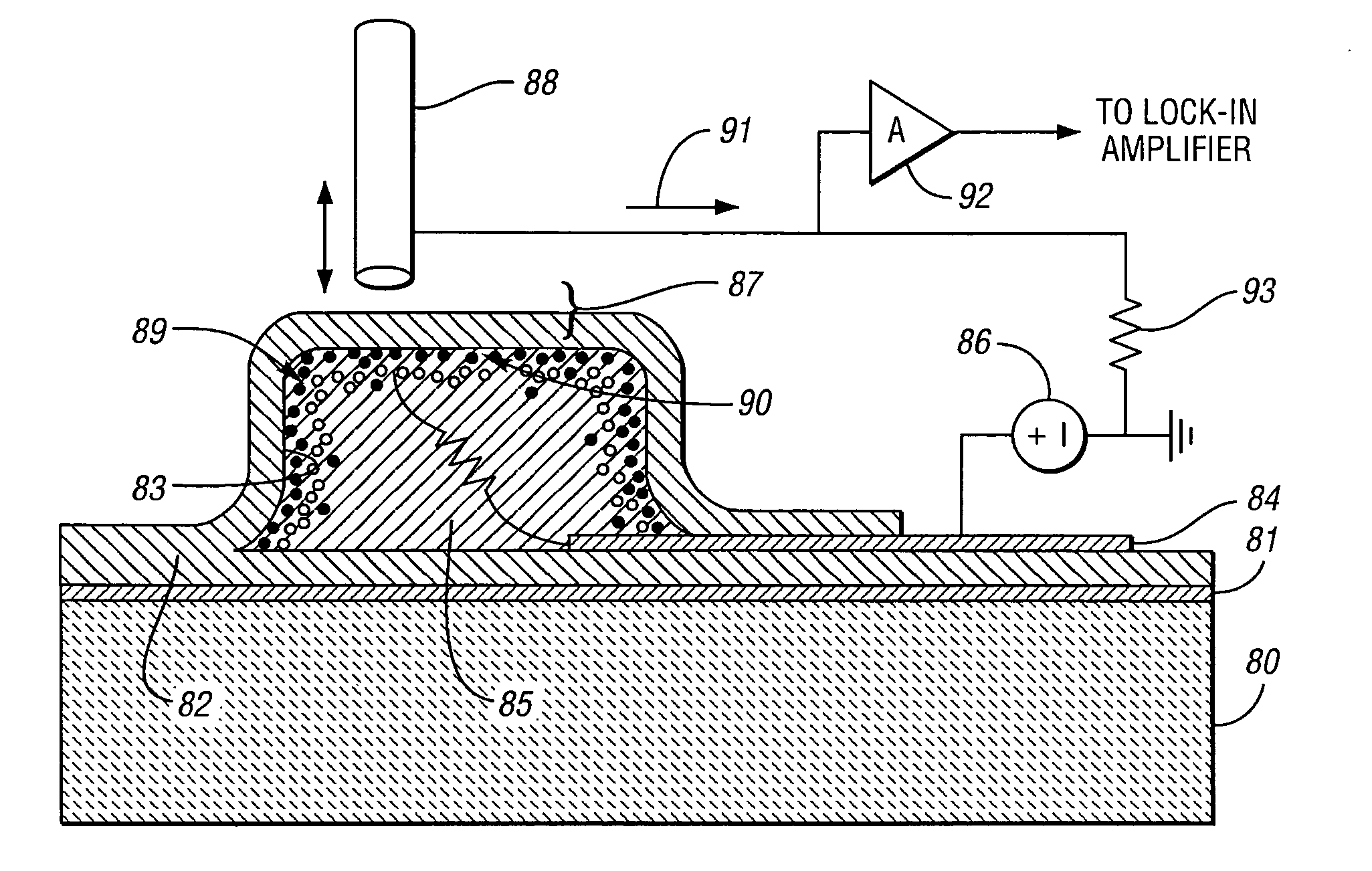
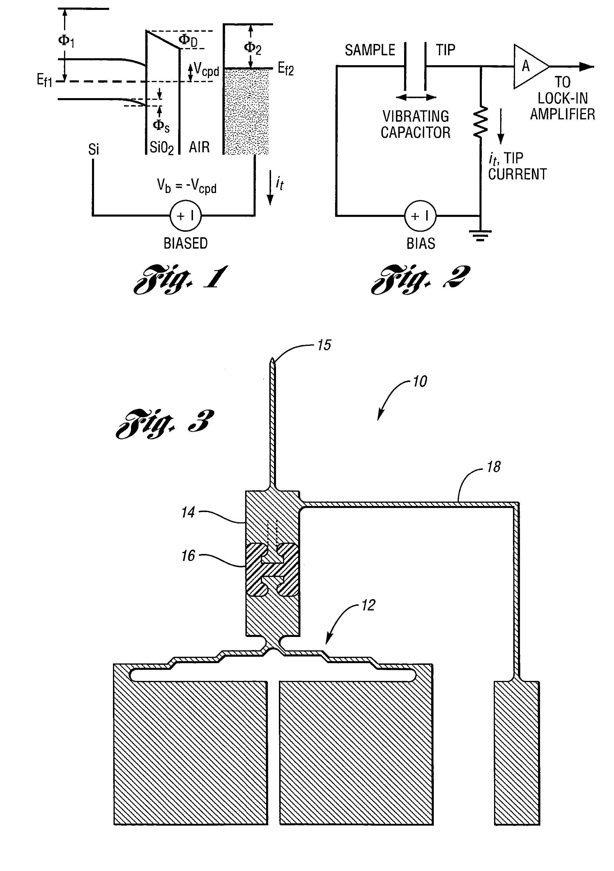
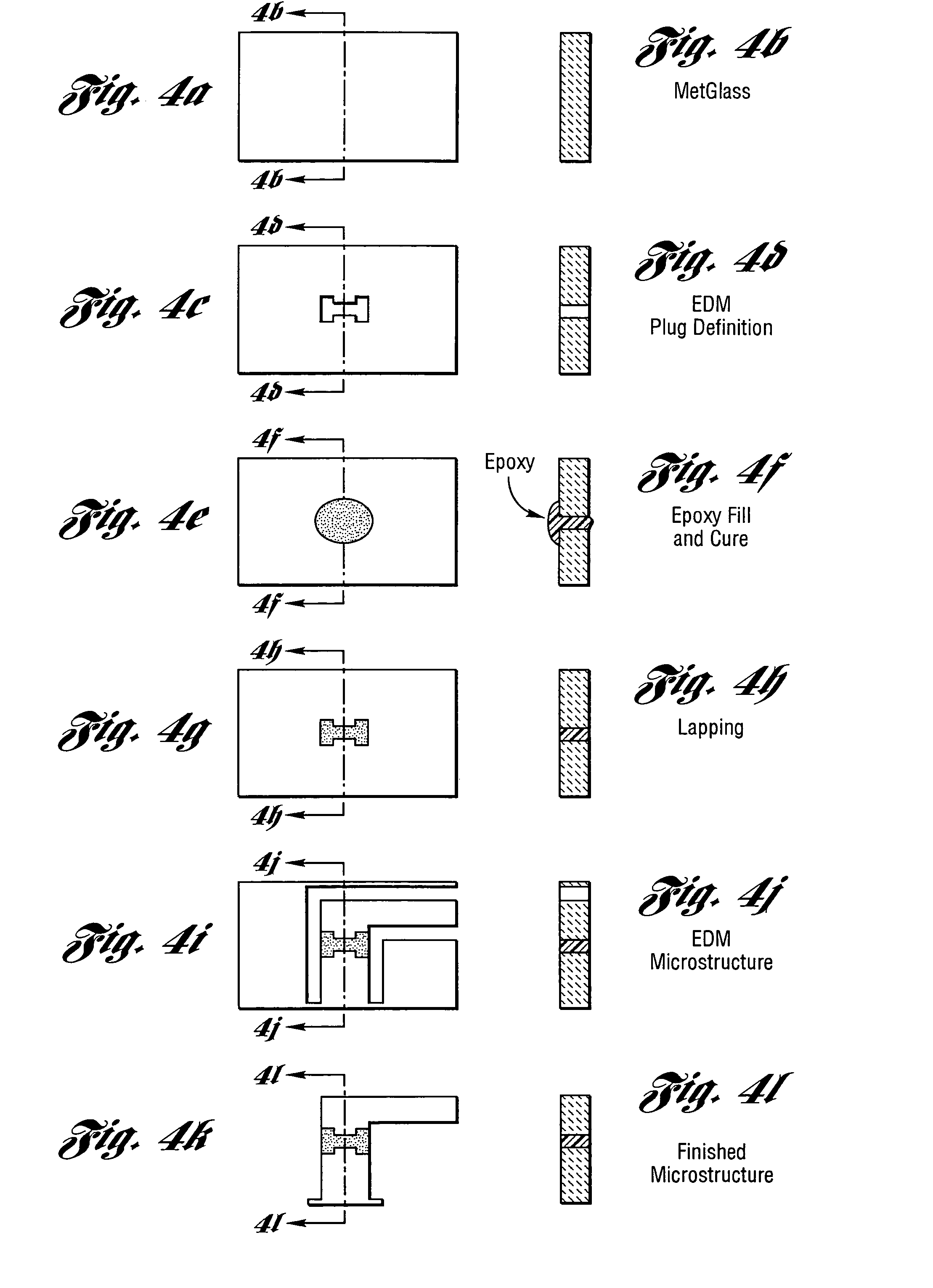
[0052]One embodiment of a micromachined probe apparatus constructed in accordance with the present invention and described herein can be used for many purposes including, but not limited to, mapping surface charge and measuring CPD. The device or apparatus generally include an actuator which provides axial dither motion, a sense probe, which is electrically isolated from the actuator, and a lead transfer beam for the probe electrode. A wide isolation region is important to minimize capacitive coupling between the drive signal of the actuator and probe. An insulating glass substrate also helps in this regard, as does the choice of actuator. The bent-beam actuator is electrothermally driven by passing current through the bent beam, which amplifies the resulting deformation into an outward motion of the probe tip [Que01]. It is selected because it offers non-resonant dither motion with amplitude in the 10 μm range with drive voltages of a few volts. The low voltage minimizes the coupli...


PUM

PropertyMeasurementUnit
thickaaaaaaaaaa
thickaaaaaaaaaa
areaaaaaaaaaaa

Abstract

A micromachined probe apparatus and methods for making and using same to characterize liquid in a fluidic channel and map embedded charge in a sample on a substrate are provided. The probe apparatus includes an integrated scanning tip and a dither actuation mechanism. The actuation is achieved using a bent-beam electrothermal actuator, and the probe tip is insulated from the actuator with a wide isolation gap. The device is fabricated by a modified micro electro-discharge machining process which allows electrical isolation within the micromachined structure using an epoxy plug. The apparatus may be used to measure changes in the external surface potential of a microfluidic channel as a function of varying pH of liquid inside the channel. The apparatus also may be used to map embedded charge in a thin layer on a substrate, showing it to be suitable for monitoring microelectronics manufacturing processes.

Description

CROSS-REFERENCE TO RELATED APPLICATION[0001]This application claims the benefit of U.S. provisional application Ser. No. 60 / 476,381, filed Jun. 6, 2003.STATEMENT REGARDING FEDERALLY SPONSORED RESEARCH OR DEVELOPEMENT[0002]This invention was made with Government support from DARPA under Grant No. 040074 and from NSF under Grant Nos. 043898 and DMR-0084402. The Government has certain rights in the invention.BACKGROUND OF THE INVENTION[0003]1. Field of the Invention[0004]This invention relates to a micromachined probe apparatus and methods for making and using same to characterize liquid in a fluidic channel and map embedded charge in a sample on a substrate.[0005]2. Background Art[0006]U.S. Pat. Nos. 6,624,377 and 6,586,699 are related to the present application.[0007]The following references are referred to in this specification:[0008][And52]J. R. Anderson et al., “Theory of the Vibrating CondenserConverter and Application to Contact PotentialMeasurements,” AUSTRALIAN JOURNAL OF APPL...

Claims


Application Information

Patent Timeline
Patent Type & Authority Patents(United States)
IPC IPC(8): G01R27/26G01R31/02G01R31/302B23H9/00G01N27/00G01Q30/14G01Q60/30G01Q60/40
CPCB23H9/00B82Y35/00G01N27/002G01Q30/14G01Q60/30G01Q60/40
Inventor GIANCHANDANI, YOGESH B.CHU, LARRY L.TAKAHATA, KENICHISELVAGANAPATHY, PONNAMBALAMSHOHET, JUDA L.
Owner WISCONSIN ALUMNI RES FOUND
Why Eureka
Try Eureka