Optical module and manufacturing method of the same, optical communication device, opto-electrical hybrid integrated circuit, circuit board, and electronic apparatus

Active Publication Date: 2006-10-10
SEIKO EPSON CORP
View PDF41 Cites 70 Cited by
  • Summary
  • Abstract
  • Description
  • Claims
  • Application Information

AI Technical Summary

Benefits of technology

[0021]Furthermore, the optical module may further include a pressing device to press the optical plug to the other surface side of the transparent substrate. As for the pressing device, for example, a leaf spring can be used. This can make a position of the optical plug in the vertical direction (orthogonal direction with respect to the transparent substrate) more stable.
[0022]Furthermore, the above-described guide surfaces may include two surfaces which are substantially parallel to each other and substantially orthogonal to the other surface of transparent substrate, and include one surface which is substantially parallel to the other surface of the transparent substrate. These surfaces and the other surface of the transparent substrate enable the optical plug to be positioned precisely.
[0023]Furthermore, the above-described guide surfaces may include two surfaces substantially orthogonal to each other and arranged at an angle of substantially 45 degrees with respect to the other surface of the transparent substrate. In addition, in this case, each of the two surfaces m

Problems solved by technology

In recent years, a signal transfer rate between circuit chips included in various devices, or between circuit boards has increased, and problems such as crosstalk between signal lines, noise radiation, impedance mismatch and high power consumption have become critical.
In case of optical connectors described in Japanese laid-open patent publication No. 7-49437, when one connector is provided with a fitting pin and the other connec

Method used


Image

  • Optical module and manufacturing method of the same, optical communication device, opto-electrical hybrid integrated circuit, circuit board, and electronic apparatus
  • Optical module and manufacturing method of the same, optical communication device, opto-electrical hybrid integrated circuit, circuit board, and electronic apparatus
  • Optical module and manufacturing method of the same, optical communication device, opto-electrical hybrid integrated circuit, circuit board, and electronic apparatus

Examples


first exemplary embodiment

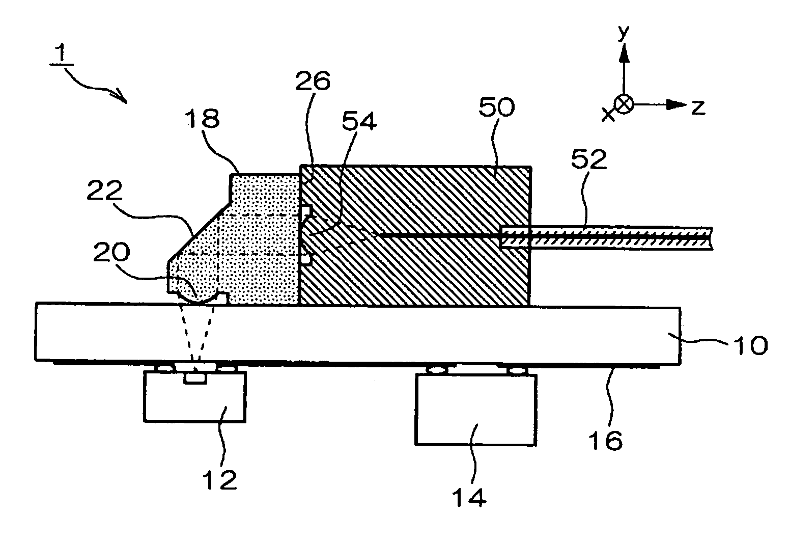
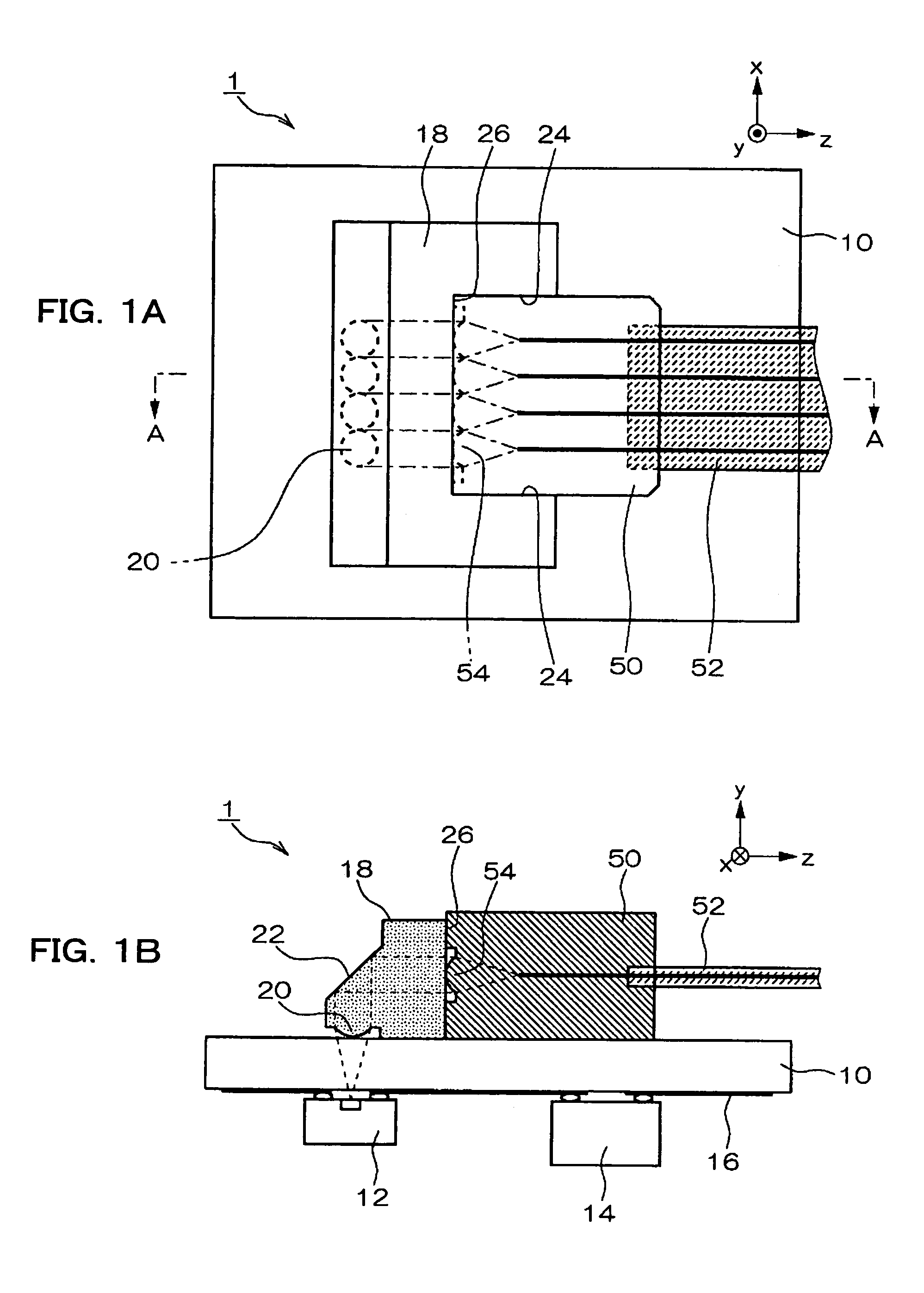
[0046]FIGS. 1(A) and 1(B) are views illustrating a configuration of an optical module according to a first exemplary embodiment. FIG. 1(A) is a plan view of the optical module according to the present exemplary embodiment. FIG. 1(B) is a cross sectional view taken along the plane A—A of FIG. 1(A). An optical module 1 shown in FIGS. 1(A) and 1(B) is mounted with an optical plug 50, which is provided at one end of a tape fiber 52 serving as an optical transmission path, and transmits and receives signal light via the tape fiber 52 for information communication. The optical module 1 includes a transparent substrate 10, an optical element 12, an electronic circuit 14, a wiring layer 16, an optical socket 18, a lens 20, and a reflective portion 22.

[0047]The transparent substrate 10 has light transmittance property with respect to the wavelength of used light and supports each element constituting the optical module 1. For example, in the case where the wavelength of light emitted from, o...

second exemplary embodiment

[0065]FIGS. 5(A) and 5(B) are views illustrating a configuration of an optical module according to a second exemplary embodiment. FIG. 5(A) is a plan view of the optical module of the present exemplary embodiment. FIG. 5(B) is a cross sectional view taken along the plane B—B of FIG. 5(A). An optical module 1a shown in the figures basically has a similar configuration to that of the optical module 1 according to the first exemplary embodiment, and common components are indicated by the same reference numerals and signs. Hereinafter, differences will be mainly described.

[0066]In the optical module 1a shown in FIGS. 5(A) and 5(B), an optical socket 18a, to which the optical plug 50 is attached, has a different shape from that of the first exemplary embodiment. The optical socket 18a includes the surfaces 24 and the surface 26 serving as guide surfaces similarly to the optical socket 18, further including a surface 32 for positioning in the Y axis direction of the optical module 1a. The...

third exemplary embodiment

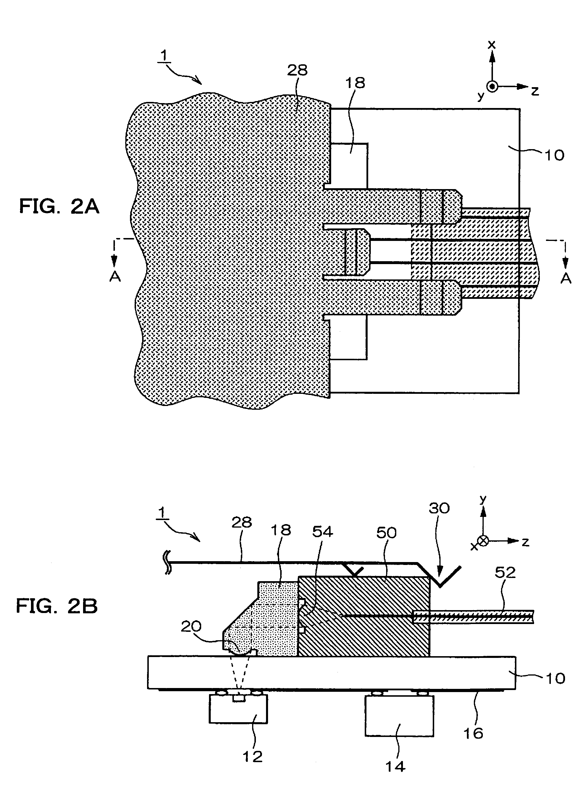
[0068]FIGS. 6(A) and 6(B) are views illustrating a configuration of an optical module according to a third exemplary embodiment. FIG. 6(A) is a plan view of the optical module of the present exemplary embodiment. FIG. 6(B) is a cross sectional view taken along the plane C—C of FIG. 6(A). An optical module 1b shown in the figures has a similar configuration to that of the above-described optical modules, and common components are indicated by the same reference numerals and signs. Hereinafter, differences will be mainly described.

[0069]In the optical module 1b shown in FIGS. 6(A) and 6(B), the optical socket 18b, to which the optical plug 50 is attached, has a different shape from those of the above-described exemplary embodiments. An optical socket 18b according to the present exemplary embodiment has surfaces 24a, a surface 26a and a surface 32a serving as guide surfaces. Respective functions of the surfaces 24a, 26a and 32a are similar to those of the above-described surfaces 24, ...


PUM


Abstract

To provide an optical module capable of miniaturization, the optical module, to which an optical plug provided at one end of an optical transmission path is attached, so as to transmit and receive signal light via the optical transmission path for information communication, includes: a transparent substrate having light transmittance property with respect to a wavelength of used signal light; an optical socket, which is arranged on one surface side of the transparent substrate and to which the optical plug is attached; an optical element, which is arranged on the other surface side of the transparent substrate and emits the signal light to the one surface side of the transparent substrate according to a supplied electrical signal, or generates an electrical signal according to the intensity of the signal light supplied from the other surface of the transparent substrate; and a reflective portion, which is arranged on the other surface of the transparent substrate and changes a path of the signal light emitted from the optical element at substantially 90 degrees to guide it to the optical transmission path, or changes a path of the signal light emitted from the optical transmission path at substantially 90 degrees to guide it to the optical element.

Description

BACKGROUND OF THE INVENTION[0001]1. Field of Invention[0002]The present invention relates to a device, components, or the like for use in information communication (signal transmission) by optical signals between a plurality of devices or inside of a device.[0003]2. Description of Related Art[0004]In recent years, a signal transfer rate between circuit chips included in various devices, or between circuit boards has increased, and problems such as crosstalk between signal lines, noise radiation, impedance mismatch and high power consumption have become critical. Consequently, optical communication has started to be introduced in signal transmission between circuit chips inside of a device, between modules or the like. Therefore, a technique of transmitting an optical signal via an optical transmission path, such as optical fiber (tape fiber) or optical waveguide for communication in place of a conventional method of transmitting an electrical signal via metal wiring has been employe...

Claims


Application Information

Patent Timeline
IPC IPC(8): G02B6/36G02B6/38G02B6/42
CPCG02B6/4214G02B6/4292G02B6/3839G02B6/3845G02B6/4249
Inventor NAGASAKA, KIMIOKANEKO, TAKEOMIYAMAE, AKIRA
Owner SEIKO EPSON CORP
Why Eureka
Try Eureka