
Memory array with surrounding gate access transistors and capacitors with global and staggered local bit lines

Active Publication Date: 2006-10-10
MICRON TECH INC
View PDF36 Cites 97 Cited by
  • Summary
  • Abstract
  • Description
  • Claims
  • Application Information

AI Technical Summary

Benefits of technology

[0013]Thus, various embodiments provide a memory array including access transistors over buried local data/bit lines which include substantially surrounding gate structures which provide improved sub-threshold performance and relatively high device density. Low resistance global data/bit lines can be selectively interconnected to the local data/bit lines to provide lower resistance paths between memory cells and sense amplifiers. Certain embodiments provide th

Problems solved by technology

Ongoing scaling of metal oxide semiconductor field effect transistor (MOSFET) technology to the deep sub-micron region where channel lengths are less than 0.1 micron (100 nanometers or 1,000 Å) causes significant problems in conventional transistor structures.
Such shallow junctions are difficult to form by conventional implantation and diffusion techniques.
Sub-threshold conduction is particularly problematic in dynamic random access memory (DRAM), as it significantly reduces the charge storage retention time of the capacitor cells.
Extremely high doping level generally results in increased leakage and reduced carrier mobility, thus making the channel shorter to improve performance, is offset or negated by the lower carrier mobility and higher leakage.
This leakage current is a significant concern and problem in low voltage and low power battery operated complimentary metal oxide semiconductor (CMOS) circuits and systems, particularly in DRAMs.
This is shown in FIG. 2 that if low voltages are used for this low power operation, then there is a problem with threshold voltages and standby leakage current being of large enough value to degrade overall circuit performance.

Method used


Image

  • Memory array with surrounding gate access transistors and capacitors with global and staggered local bit lines
  • Memory array with surrounding gate access transistors and capacitors with global and staggered local bit lines
  • Memory array with surrounding gate access transistors and capacitors with global and staggered local bit lines

Examples


Embodiment Construction

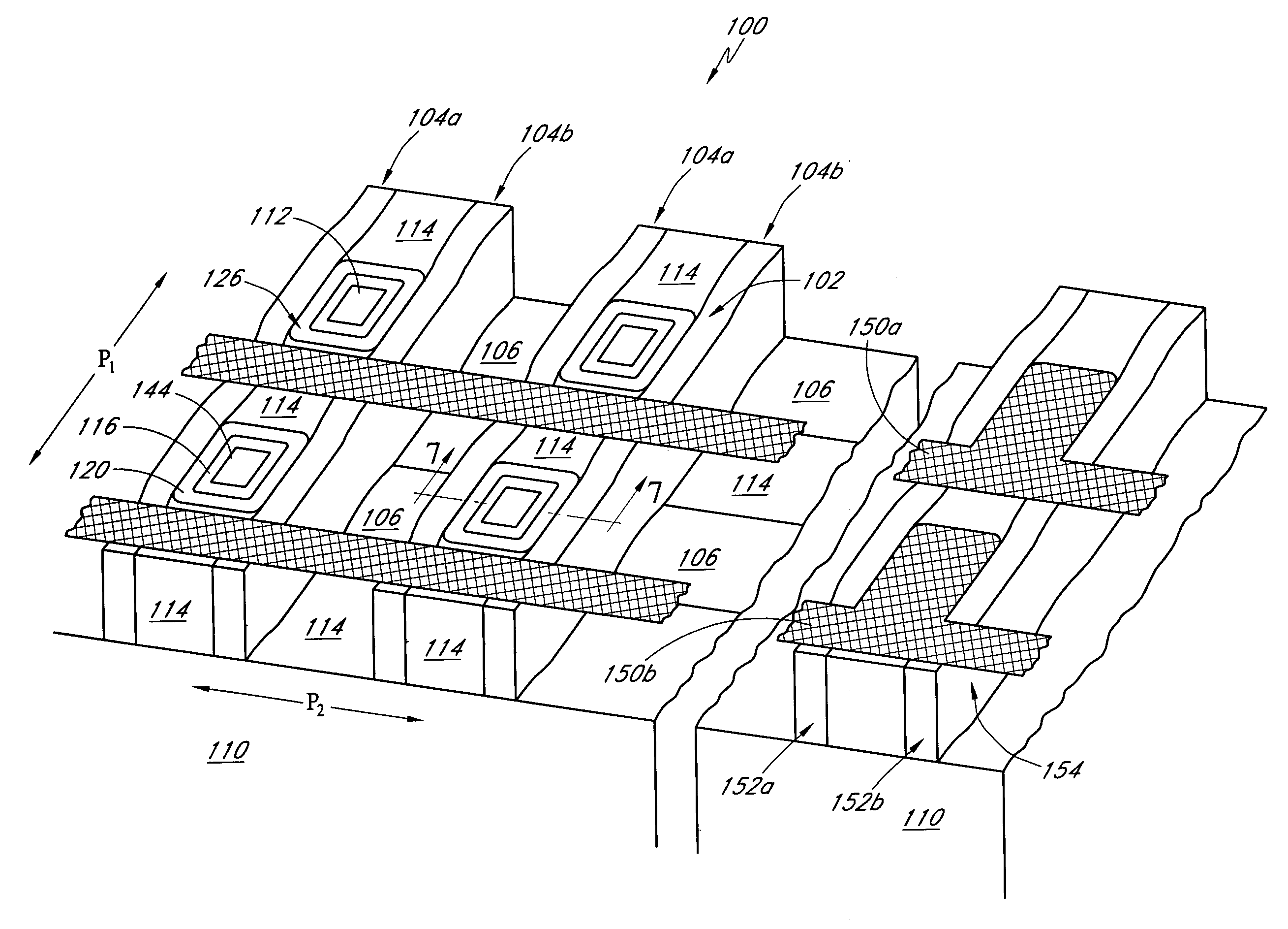
[0031]Reference will now be made to the drawings of the various embodiments of the invention wherein like reference numerals will refer to like parts / structures throughout. FIGS. 5A, 5B, and 6 illustrate a top section view, side section view, and perspective view respectively of embodiments of a memory circuit access array 100, which in following will be referred to as the array 100 for brevity. The array 100 provides access with a plurality of memory cells 101, in certain embodiments an array of DRAM cells, which can be utilized for storage and access of information (FIG. 24). The array 100 comprises a plurality of cell access transistors 102 which are interconnected with corresponding charge storage devices to define the memory cells 101 in a memory array 170 (FIG. 24). In one embodiment, the charge storage devices comprise storage capacitors 103. Each of the access transistors 102 are in electrical communication with a corresponding word line 104 and local data / bit line 106. In t...


PUM


Abstract

A memory array with staggered local data / bit lines extending generally in a first direction formed in an upper surface of a substrate and memory cell access transistors extending generally upward and aligned generally atop a corresponding local data / bit line. Selected columns of the memory cell access transistors are sacrificed to define local data / bit access transistors which are interconnected with overlying low resistance global data / bit lines. The global data / bit lines provide selectable low resistance paths between memory cells and sense amplifiers. The sacrificed memory cell access transistors and staggered local data / bit lines provide increased footprints for sense amplifiers to facilitate increased circuit integration.

Description

BACKGROUND OF THE INVENTION[0001]1. Field of the Invention[0002]The invention relates to the field of high density semiconductor memory arrays and more particularly to arrays with vertical transistors having sub-photolithographic device dimensions with ultra-thin pillars and substantially fully surrounding gates suitable for use as access transistors, such as for DRAM arrays. The arrays include additional room for access transistors and have high density local bit / data lines as well as low resistance global bit / data lines.[0003]2. Description of the Related Art[0004]Ongoing scaling of metal oxide semiconductor field effect transistor (MOSFET) technology to the deep sub-micron region where channel lengths are less than 0.1 micron (100 nanometers or 1,000 Å) causes significant problems in conventional transistor structures. Generally, junction depth should be much less than the channel length, and thus for a channel length of, for example 1,000 Å, this implies junction depths on the o...

Claims


Application Information

Patent Timeline
IPC IPC(8): G11C11/24H01L27/108
CPCG11C7/18H01L27/10876H01L29/66477G11C2207/002H10B12/053
Inventor FORBES, LEONARD
Owner MICRON TECH INC
Features
  • Generate Ideas
  • Intellectual Property
  • Life Sciences
  • Materials
  • Tech Scout
  • Unparalleled Data Quality
  • Higher Quality Content
  • 60% Fewer Hallucinations
Learn More