Method for fabricating semiconductor device

a semiconductor and device technology, applied in the direction of semiconductor devices, basic electric elements, electrical equipment, etc., can solve the problems of excessive etching process, damage to an insulation layer, and formation of electric leakage current paths, etc., to prevent defect generation

Inactive Publication Date: 2006-10-17
SK HYNIX INC
View PDF5 Cites 28 Cited by
  • Summary
  • Abstract
  • Description
  • Claims
  • Application Information

AI Technical Summary

Benefits of technology

[0033]It is, therefore, an object of the present invention to provide a method for fabricating a semiconductor device capable of preventing defect generation resulting from deterioration of a property of insulation during a cleaning process for expanding a contact opening unit.

Problems solved by technology

During the SAC etching process, the etching process is excessively performed since there are many portions to be etched back.
Therefore, the damage is taken place on an insulation layer being made up of the oxide-based material having a weak etching tolerance to the HF or the BOE.
And as a property of insulation is deteriorated, an electric leakage current path is also formed.

Method used


Image

  • Method for fabricating semiconductor device
  • Method for fabricating semiconductor device
  • Method for fabricating semiconductor device

Examples


Embodiment Construction

[0039]A method for fabricating a semiconductor device in accordance with a preferred embodiment of the present invention will be described in detail with reference to the accompanying drawings.

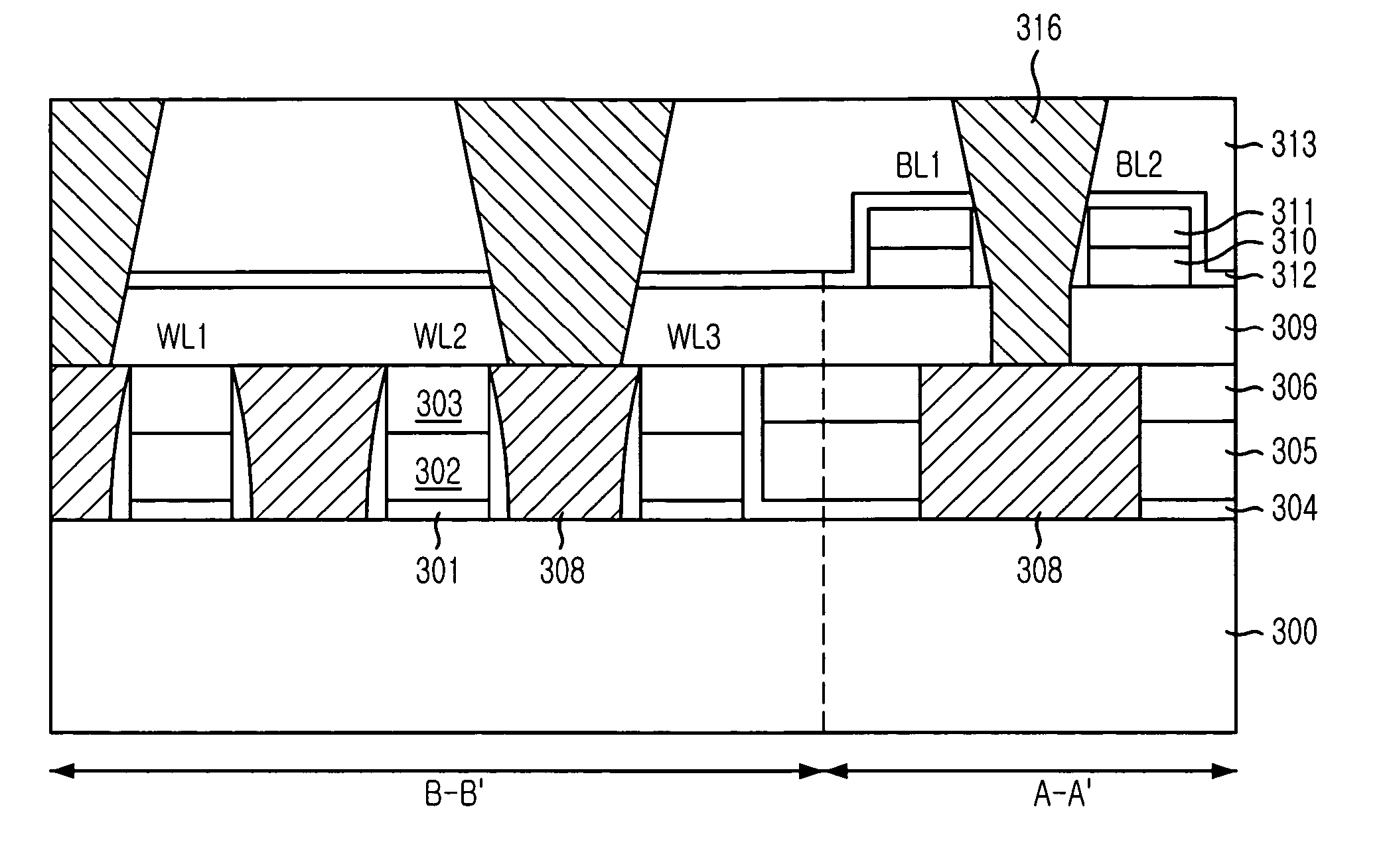
[0040]FIGS. 3A to 3E are cross-sectional views illustrating a storage node contact forming process of a semiconductor device in accordance with a preferred embodiment of the present invention. The above cross-sectional views are taken along directions of lines A–A′ and B–B′, respectively. Referring to FIGS. 3A to 3E, the storage node contact forming process in accordance with a preferred embodiment of the present invention is explained in detail, hereinafter.

[0041]FIG. 3A is a cross-sectional view illustrating a photoresist pattern 307 forming process as a mask for a plurality of isolated cell contacts.

[0042]First, a gate insulation layer 301, a gate conductive layer 302 and a gate hard mask 303 are sequentially deposited on a substrate 300 provided with various device elements. Thereafter, a ...


PUM


Abstract

Disclosed is a method for fabricating a semiconductor device with an improved process margin obtained by preventing damage to an inter-layer insulation layer during a wet cleaning process. Particularly, the method includes the steps of: forming a plurality of a first conductive pattern having a stack pattern of a first conductive and a first hard mask; forming a first inter-layer insulation layer of a good gap-fill property with a height between the first conductive material and the first hard mask on the first conductive layer; forming a second inter-layer insulation layer; forming a second conductive layer contacted the first conductive layer between the plurality of the first conductive patterns as passing through the first and the second inter-layer insulation layers; forming a third inter-layer insulation layer; forming a plurality of second conductive patterns; forming a fourth inter-layer insulation layer; and forming a third conductive layer contacted to the second conductive layer.

Description

FIELD OF THE INVENTION[0001]The present invention relates to a method for fabricating a semiconductor device; and particularly to a method for fabricating a semiconductor device capable of preventing a damage on a bottom conductive pattern during a contact forming process and increasing a process margin by preventing a damage on an inter-layer insulation layer induced by a wet cleaning solution during a storage node contact opening process.DESCRIPTION OF RELATED ARTS[0002]A lot of efforts have been made in many ways to obtain a high integration and a high capability of a semiconductor device. Among those efforts, a secure of a contact region according to the contact formation is one of the essential technologies for the high integration of the semiconductor device.[0003]FIG. 1 is a top view illustrating a lay out of an IT cell of a semiconductor memory device.[0004]Referring to FIG. 1, a plurality of electrodes, i.e., a plurality of word lines WL1, WL2 and WL3 are placed in a same d...

Claims


Application Information

Patent Timeline
Patent Type & Authority Patents(United States)
IPC IPC(8): H01L21/4763H01L21/28H01L21/306H01L21/311H01L21/44H01L21/60H01L21/768H01L29/00
CPCH01L21/31116H01L21/76802H01L21/76829H01L21/76897H01L21/02052Y10S438/97H01L21/28
Inventor LEE, SUNG-KWONJUNG, TAE-WOO
Owner SK HYNIX INC
Why Eureka
Try Eureka