Multi-junction photovoltaic cell having buffer layers for the growth of single crystal boron compounds

a photovoltaic cell and multi-junction technology, applied in the field of photovoltaic cells, can solve the problems of increasing the cost of a launch more than linearly, increasing the cost of a launch, and increasing the cost per watt of electrical power generation capacity of photovoltaic systems

Inactive Publication Date: 2006-10-17
THE BOEING CO
View PDF15 Cites 124 Cited by
  • Summary
  • Abstract
  • Description
  • Claims
  • Application Information

AI Technical Summary

Problems solved by technology

The interest in photovoltaic (PV) cells or solar cells has been increasing due to concerns regarding pollution and limited available resources.
An increased payload can increase the cost of a launch more than linearly.
The cost per watt of electrical power generation capacity of photovoltaic systems is a main factor that inhibits their widespread use in terrestrial applications.
For a multiple-cell PV device, efficiency is limited by the requirement of low resistance interfaces between the individual cells to enable the generated current to flow from one cell to the next.
limitation of such triple-junction solar cells includes the inability of increasing the AMO efficiency above 29.3% (to, for example, 35% or higher). T
Limitations of such materials include a lack of a bandgap around 1.0 eV that may be lattice matched to Ge and a lack of requisite material properties needed to process a solar cell.
Some materials such as Gallium Indium Arsenic Nitride (GaInAsN) have been used in an attempt to achieve lattice-matching characteristics, however an ability to produce material with requisite characteristics and with a bandgap around 1.0 eV has not been achieved.
Prior art methods to grow epitaxial single crystal boron compounds, such as those from National Renewable Energy Laboratories (NREL), have followed conventional MOCVD growth techniques to achieve a low boron content of about 1.6% and could not demonstrate lattice matched boron based materials (such as BGaInAs) with high boron content due to a reaction between indium and boron source gases during the growth of the boron based layer.
None of these techniques, however, could form epitaxial boron compounds.
Utilizing such a traditional method, NREL could not achieve a preferred composition (B0.093 Ga0 707 In0 2 As, further described below) in the BGaInAs layer to produce an about 1.0 eV bandgap due to crystallization problems in enhancing the boron content as well as the pre-reaction problems associated with the source materials.
However, because the traditional growth method was utilized, the required composition of BGaInAs material to achieve an about 1.0 eV bandgap was not realized.

Method used


Image

  • Multi-junction photovoltaic cell having buffer layers for the growth of single crystal boron compounds
  • Multi-junction photovoltaic cell having buffer layers for the growth of single crystal boron compounds
  • Multi-junction photovoltaic cell having buffer layers for the growth of single crystal boron compounds

Examples


Embodiment Construction

[0033]The following detailed description is of the best currently contemplated modes of carrying out the invention. The description is not to be taken in a limiting sense, but is made merely for the purpose of illustrating the general principles of the invention, since the scope of the invention is best defined by the appended claims.

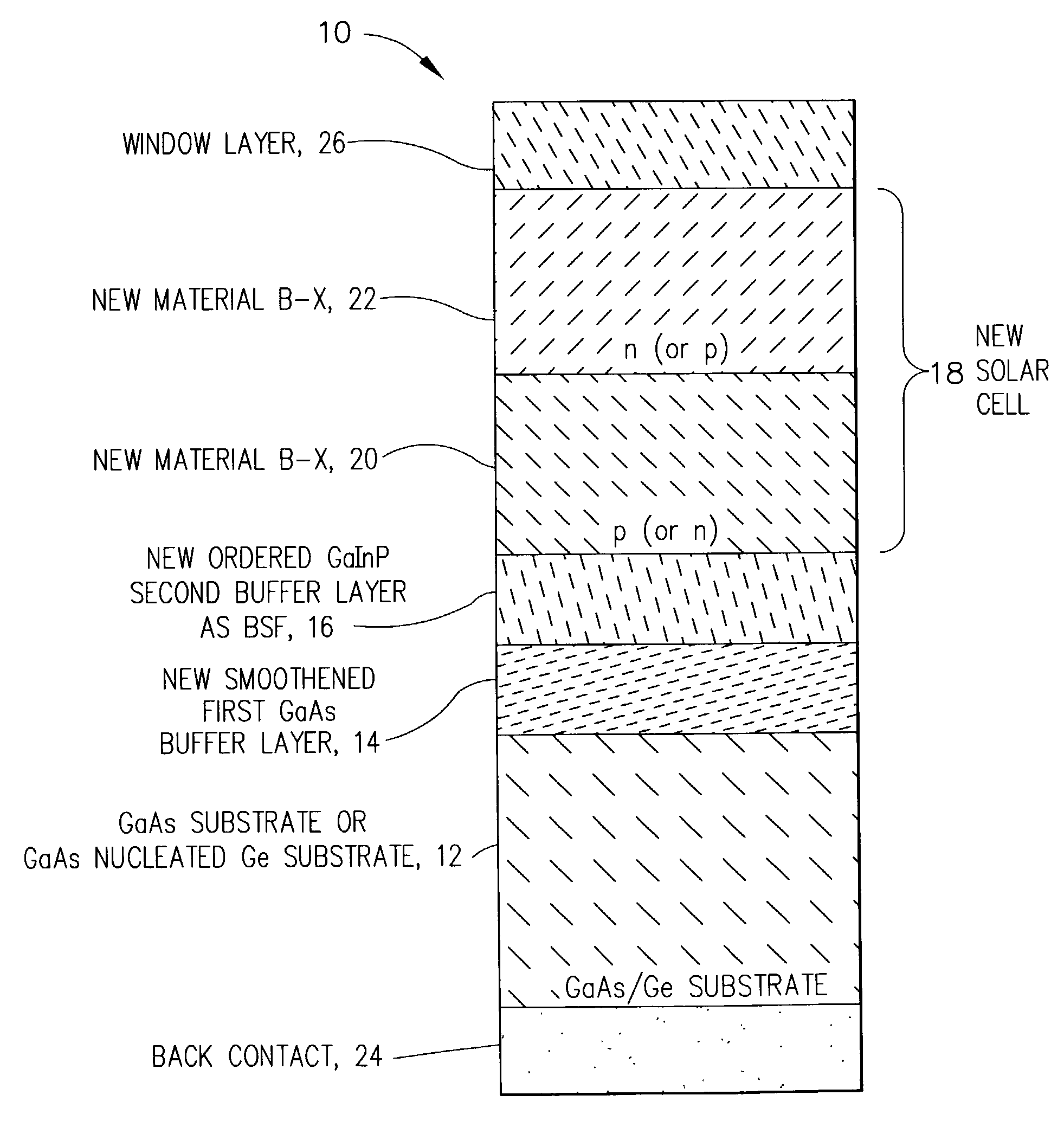
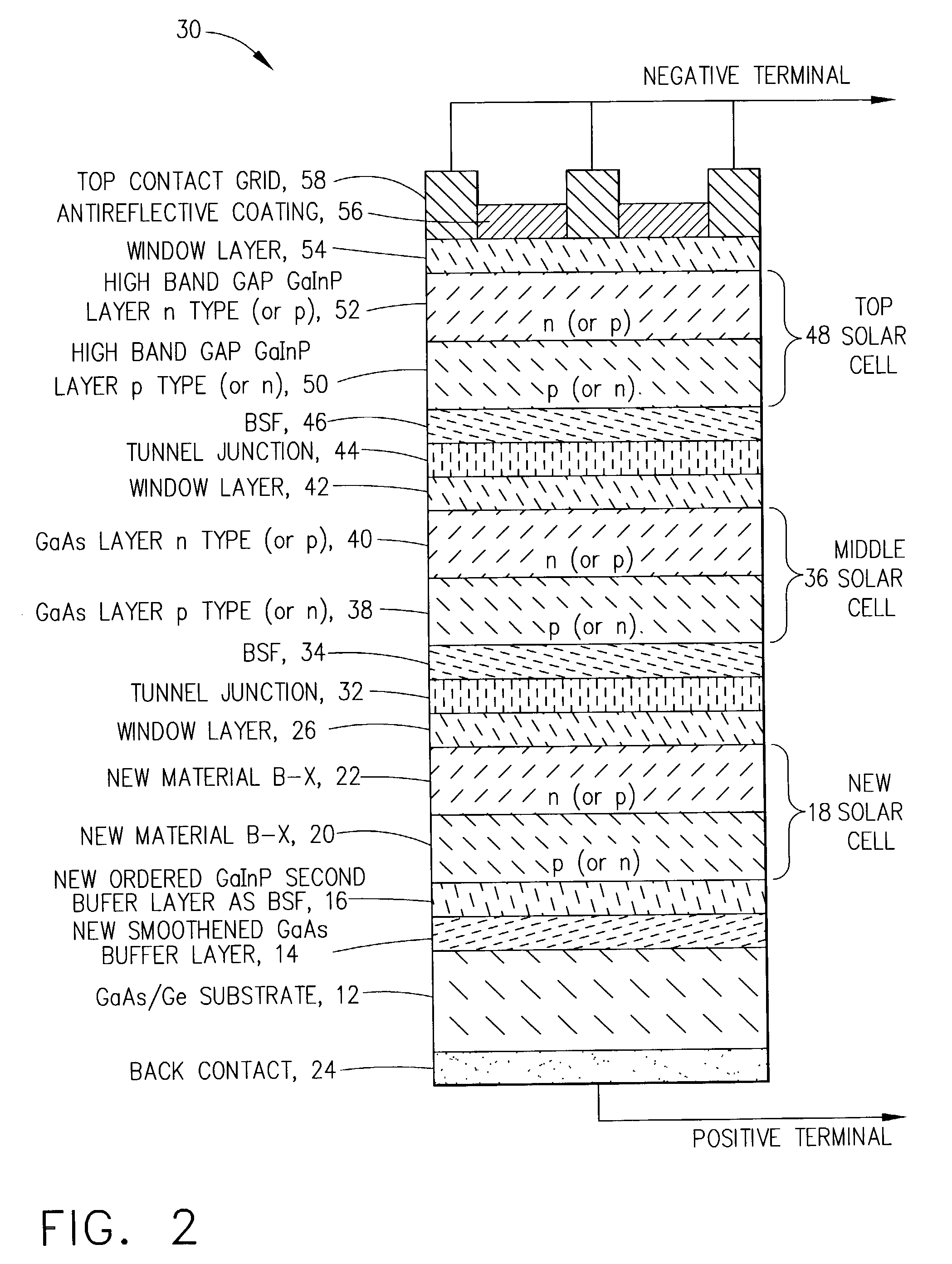
[0034]The present invention generally provides two novel buffer layers prior to the growth of boron-containing compounds such as BGaAs, BGaInAs, and BGaAsSb. One of the buffer layers may be atomically smooth while the other buffer layer may be atomically ordered. An atomically smooth buffer layer can be grown at a first temperature, annealed at a higher temperature, and then cooled at the first temperature, for example. Such an annealing process allows various materials (for example, Ga and As) within the buffer layer to be grown smoothly such that their atomic bonds are properly maintained and contain fewer crystal defects.

[0035]An atomically ordered b...


PUM


Abstract

The present invention provides a solar cell comprising a substrate, a first buffer layer disposed above the base layer, a second buffer layer disposed above the first buffer layer, a first boron compound layer disposed above the second buffer layer, a second boron compound layer disposed above the first compound layer, and a window layer disposed above the second compound layer, wherein the first compound layer comprises a first type of doping, wherein the second compound layer comprises a second type of doping, wherein the second buffer layer comprises a higher energy bandgap than the first compound layer, and wherein the first buffer layer and the second buffer layer permit a boron content in the first compound layer and the second compound layer to be greater than 3 %.

Description

BACKGROUND OF THE INVENTION[0001]The present invention generally relates to photovoltaic cells and, more specifically, to an enhanced multi-junction photovoltaic cell that includes buffer layers for the growth of single crystal boron compounds.[0002]The interest in photovoltaic (PV) cells or solar cells has been increasing due to concerns regarding pollution and limited available resources. This interest includes both terrestrial and non-terrestrial applications. In the non-terrestrial environment of outer space, the concern over limited resources of any type is a major one because the need to increase an amount of a resource increases a spacecraft's payload. An increased payload can increase the cost of a launch more than linearly. With the ready availability of solar energy in outer space for a spacecraft, such as a satellite, the efficient conversion of solar energy into electrical energy is an obvious alternative to an increased payload.[0003]The cost per watt of electrical powe...

Claims


Application Information

Patent Timeline
Patent Type & Authority Patents(United States)
IPC IPC(8): H01L31/04H01L31/06H01L31/00H01L31/0304H01L31/0687H01L31/0693
CPCH01L31/03046H01L31/0687H01L31/0693Y02E10/544
Inventor NARAYANAN, AUTHI A.SCHWARTZ, JOEL A.
Owner THE BOEING CO
Why Eureka
Try Eureka