Method and apparatus for minimizing threshold variation from body charge in silicon-on-insulator circuitry

a silicon-on-insulator and threshold variation technology, applied in the field of silicon-on-insulator (soi) cmos circuitry, can solve the problems of high bit-error rate, pulse width distortion, pulse distortion shown in trace b

Active Publication Date: 2006-10-31
MARVELL ASIA PTE LTD
View PDF4 Cites 9 Cited by
  • Summary
  • Abstract
  • Description
  • Claims
  • Application Information

AI Technical Summary

Problems solved by technology

Either of these communications systems may be implemented using SOI technology which give rise to the “history effect” which cause pulse width distortions.
If one logic transition to a logic state occurs with one body charge condition and the next transition occurs with another different body charge condition, then the resulting pulse width will be modified (history effect) which may lead to timing errors.
However, in SOI technology, the first logic transition is delayed (T prop+T hist) whereas the second consecutive logic transition is delayed by only T prop resulting in the pulse distortion shown in trace 203FIG. 2.
This amount of pulse distortion along with the uncertainties of jitter and latch setup / hold times will result in high bit-error rates if un-compensated.
However, this solution requires far more power and is thus less efficient requiring more power which is exacerbated by high frequency.

Method used


Image

  • Method and apparatus for minimizing threshold variation from body charge in silicon-on-insulator circuitry
  • Method and apparatus for minimizing threshold variation from body charge in silicon-on-insulator circuitry
  • Method and apparatus for minimizing threshold variation from body charge in silicon-on-insulator circuitry

Examples


Embodiment Construction

[0016]In the following description, numerous specific details are set forth to provide a thorough understanding of the present invention. However, it will be obvious to those skilled in the art that the present invention may be practiced without such specific details. In other instances, well-known circuits may be shown in block diagram form in order not to obscure the present invention in unnecessary detail. For the most part, details concerning timing, and the like have been omitted inasmuch as such details are not necessary to obtain a complete understanding of the present invention and are within the skills of persons of ordinary skill in the relevant art.

[0017]Refer now to the drawings wherein depicted elements are not necessarily shown to scale and wherein like or similar elements are designated by the same reference numeral through the several views.

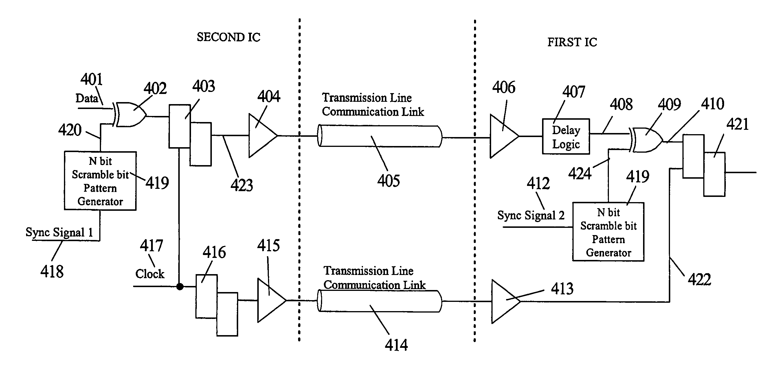
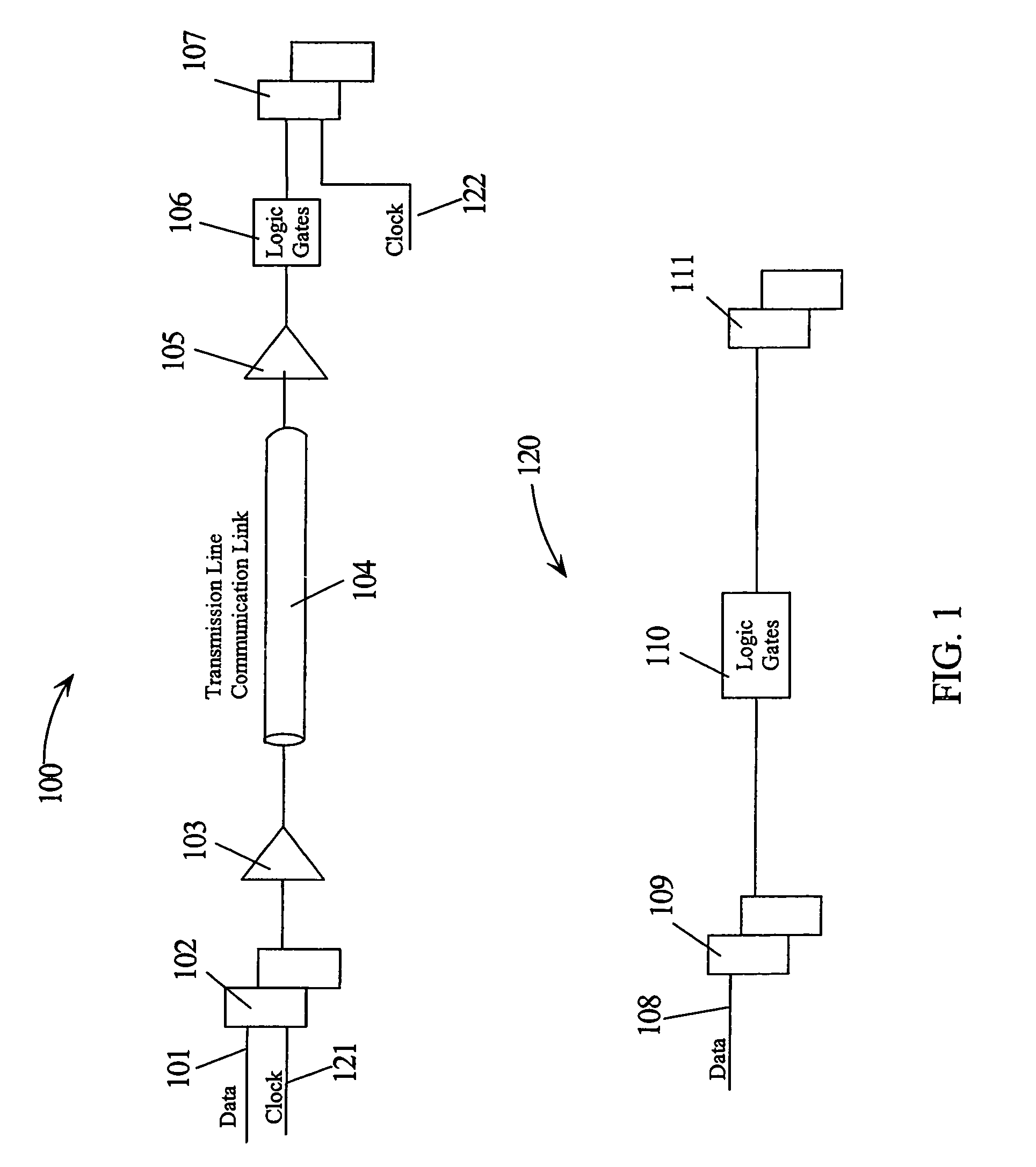
[0018]FIG. 1 illustrates a chip-to-chip communication path 100 and an intra-chip communication path 120. In the chip-to-chip com...


PUM


Abstract

Circuitry used to de-skew data channels coupling parallel data signals over a communication link employs SOI circuitry that is subject to generating pulse distortion due to the history effect modifying threshold voltages. To substantially eliminate the pulse distortion, data signals are XOR with a repeating scramble data pattern that generates scrambled data with a minimum average ratio of logic ones to logic zeros logic zeros to logic ones. The scrambled data is sent over the communication link and de-skewed in the SOI circuitry with little or no pulse distortion. The scramble data pattern is again generated at the receiver side of the communication link after a delay time to synchronize the logic states of the scramble data pattern that generated the scrambled data with the scrambled data at the receiver side. The delayed scrambled data pattern is again XOR'ed with the scrambled data to recover the data signal.

Description

TECHNICAL FIELD[0001]The present invention relates in general to complementary metal oxide semiconductor (CMOS) circuitry and in particular to Silicon-on-Insulator (SOI) CMOS circuitry.BACKGROUND INFORMATION[0002]In a typical data communications system, data must be sent from some driving latch and captured at a receiving latch. FIG. 1 shows basic block diagrams of such a data communications system implemented as either a chip-to-chip interface 100 or an on-chip interface 120. In a chip-to-chip interface 100, various components such as off-chip drivers (e.g., 103) and receivers (e.g., 105), transmission lines (e.g., 104) (printed wiring boards and / or cables), and some amount of logic circuitry (e.g., 106) will exist in the communications path. In contrast, an on-chip interface will typically comprise only internal logic gates (e.g., 109, 110, and 111) in the communications path.[0003]Either of these communications systems may be implemented using SOI technology which give rise to th...

Claims


Application Information

Patent Timeline
Patent Type & Authority Patents(United States)
IPC IPC(8): H03M7/00
CPCH04L25/03866H04L7/0008
Inventor DREPS, DANIEL M.REESE, ROBERT J.SAENZ, HECTOR
Owner MARVELL ASIA PTE LTD
Why Eureka
Try Eureka