
Test structure and methodology for semiconductor stress-induced defects and antifuse based on same test structure

a test structure and stress-induced defect technology, applied in semiconductor/solid-state device testing/measurement, semiconductor device details, semiconductor/solid-state device testing/measurement, etc., can solve problems such as yield and reliability, degrade product functionality, and limited use of efficient and sensitive monitoring systems for stress-induced defects for both development and routine monitoring in manufacturing

Inactive Publication Date: 2006-11-07
IBM CORP
View PDF30 Cites 10 Cited by
  • Summary
  • Abstract
  • Description
  • Claims
  • Application Information

AI Technical Summary

Benefits of technology

[0008]A second aspect of the present invention is a method for detecting semiconductor process stress-induced defects comprising: providing one or more polysilicon-bounded test diodes, each polysilicon-bounded test diodes comprising a diffused first region within an upper portion of a second region of a silicon substrate, the second region of an opposite dopant type from the diffused first region, the diffused first region surrounded by a peripheral dielectric isolation and a peripheral polysilicon gate comprising a polysilicon layer over a dielectric layer, the polysilicon gate overlapping a peripheral portion of the diffused first region; stressing each the polysilicon-bounded test diode; measuring during the stressing for each the polysilicon-bounded test diode, the current through the first region as a function of a forward bias voltage applied between the first and second regions at at least a predetermined forward bias voltage; and determining the frequency distribution of the slope of the forward bias voltage versus the first region current at the pre-selected forward bias voltage for the one or more polysilicon-bounded test diodes.
[0009]A third aspect of the present invention is a method for detecting semiconductor process stress-induced defects comprising: providing one or more polysilicon-bounded test diodes, each polysilicon-bounded test diode comprising a diffused first region within an upper portion of a second region of a silicon substrate, the second region of an opposite dopant type from the diffused first region, the diffused first region surrounded by a peripheral dielectric isolation, a peripheral polysilicon gate comprising a polysilicon layer over a dielectric layer, the polysilicon gate overlapping a peripheral portion of the diffused first region; stressing each the polysilicon-bounded test diode for a pre-determined amount of time; and monitoring, after the stressing, each the polysilicon-bounded test diode for soft breakdown.

Problems solved by technology

The fabrication processes for silicon chips often lead to the formation of small stress-induced silicon defects that may coalesce into dislocations or stacking faults that degrade the product functionality, yield and reliability.
Results of stress-induced defects include gate and capacitor dielectric leakage, which may be yield or reliability defects.
While methods exists for monitoring processes for defects and other methods exist for detecting stress during processes development, an efficient and sensitive monitoring systems for detecting stress-induced defects that could be used for both development and routine monitoring in manufacturing is limited.

Method used


Image

  • Test structure and methodology for semiconductor stress-induced defects and antifuse based on same test structure
  • Test structure and methodology for semiconductor stress-induced defects and antifuse based on same test structure
  • Test structure and methodology for semiconductor stress-induced defects and antifuse based on same test structure

Examples


first embodiment

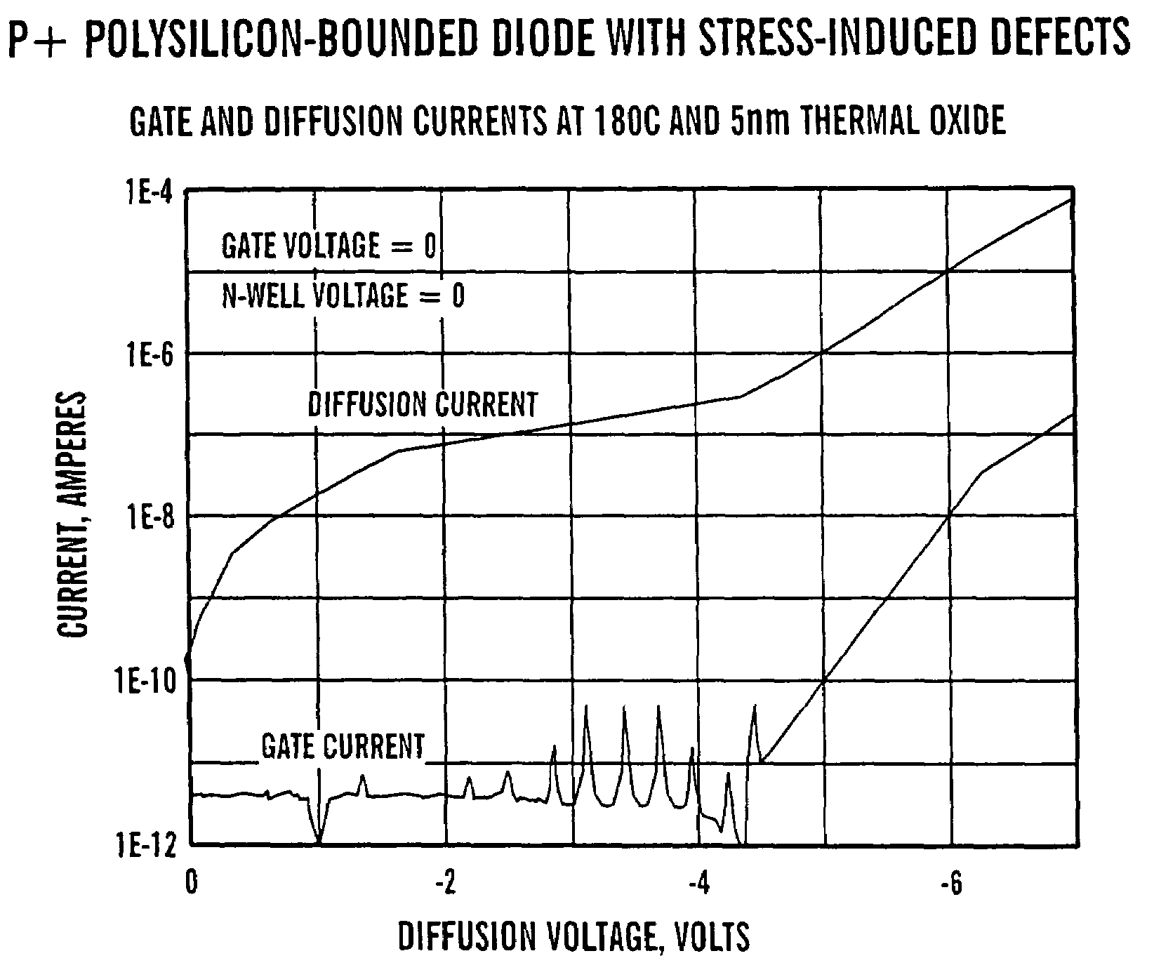
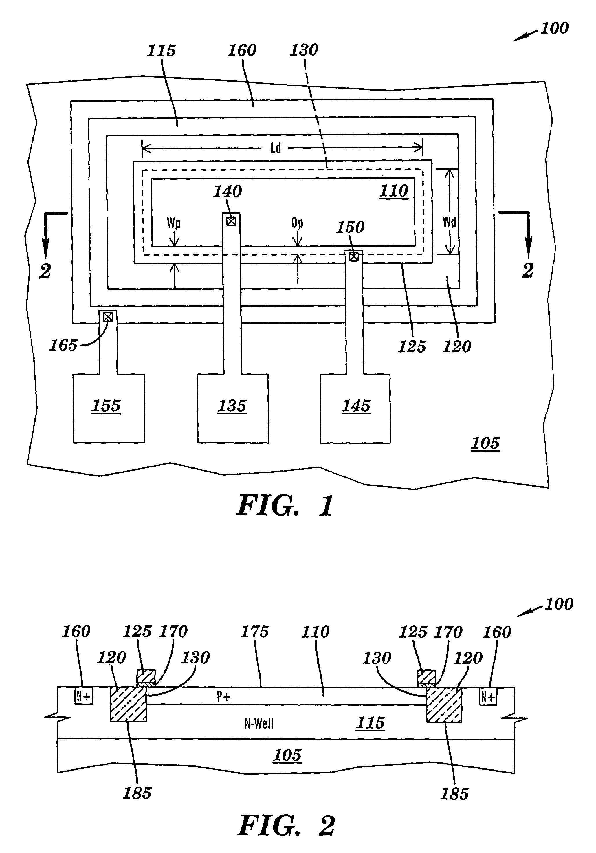
[0057]FIGS. 7A through 7C are flowcharts illustrating first, second and third test methodologies respectively, according to the present invention. Referring to FIG. 7A, in step 500, a polysilicon-bounded test diode 100 (see FIGS. 1 and 2) is selected. In step 505, polysilicon-bounded test diode 100 is maintained at a pre-selected temperature. In one example, the pre-selected temperature is 180° C. However, any temperature in the range of about 100 to 200° C. may be used. In step 510, polysilicon gate 125, N-well 115 and substrate 105 (see FIG. 1) are held at ground potential. In one example, ground potential is about 0 volts. In step 515, P+ diffusion region 110 (see FIG. 1) is ramped from about 0 volts to about −6 volts. In step 520, the current through polysilicon gate 125 (see FIG. 1) is monitored for current spikes. An example is illustrated in FIGS. 8 and 9 and described below.

[0058]Referring to FIG. 7B, in step 525, a test DRAM device 300 (see FIG. 5) is selected. In step 530,...

second embodiment

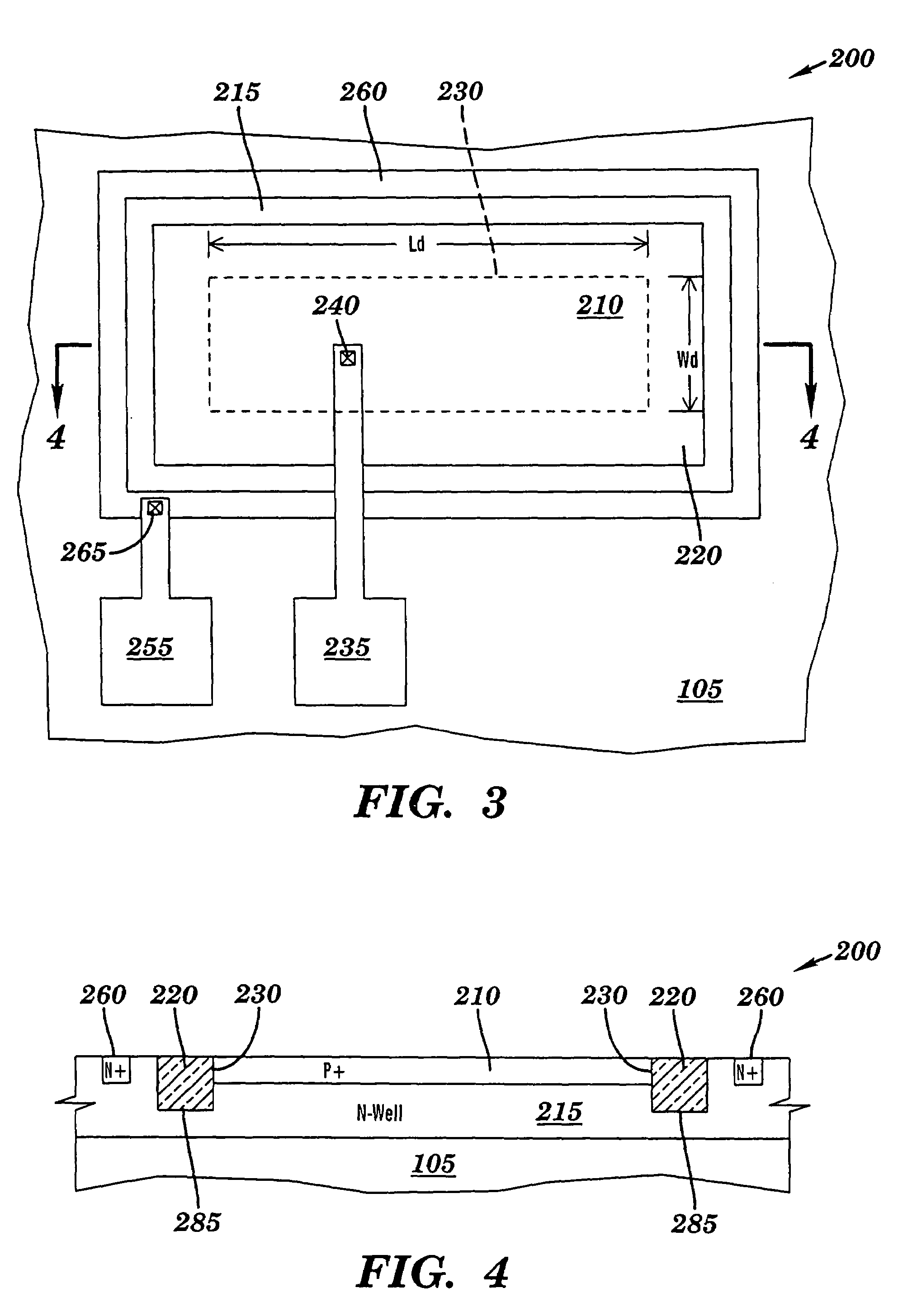
[0065]FIGS. 10A and 10B are flowcharts illustrating fourth and fifth test methodologies respectively, according to the present invention. Referring to FIG. 10A, in step 575, one or more polysilicon-bounded test diodes 100 (see FIGS. 1 and 2) is selected. In step 580, for each polysilicon-bounded test diode 100, polysilicon gate 125, N-well 115 and substrate 105 (see FIG. 1) are held at ground potential. In one example, ground potential is about 0 volts. In step 585, for each polysilicon-bounded test diode 100, P+ diffusion region 110 (see FIG. 1) is ramped from about 0 volts to about 0.85 volts. In step 590, for each polysilicon-bounded test diode 100, the current through P+ diffusion region 110 (see FIG. 1) is measured as a function of voltage and a frequency distribution analysis of the slope of the forward bias voltage / P+ diffusion current at a pre-selected forward bias voltage is performed. In step 595, one or more STI-bounded reference diodes 200 (see FIGS. 3 and 4) is selected...

third embodiment

[0080]FIGS. 13A, 13B and 13C are flowcharts illustrating sixth, seventh and eighth test methodologies respectively, according to the present invention. Referring to FIG. 13A, in step 670, one or more polysilicon-bounded test diodes 100 (see FIGS. 1 and 2) is selected. In step 675, each polysilicon-bounded test diode 100 is maintained at a pre-selected temperature. In one example, the pre-selected temperature is 160° C. However, any temperature in the range of about 100 to 200° C. may be used. In step 680, for each polysilicon-bounded test diode 100, N-well 115, substrate 105 and polysilicon gate 125 (see FIG. 1) are held at ground potential. In one example, ground potential is about 0 volts. In step 685, for each polysilicon-bounded test diode 100, a pre-determined voltage is applied to P+ diffusion region 110 (see FIG. 1) for at least a pre-determined time. In one example, the predetermined voltage is about −6.3 volts or less and the pre-determined time is about 0.5 hours or more. ...


PUM


Abstract

A method for detecting semiconductor process stress-induced defects. The method comprising: providing a polysilicon-bounded test diode, the diode comprising a diffused first region within an upper portion of a second region of a silicon substrate, the second region of an opposite dopant type from the first region, the first region surrounded by a peripheral dielectric isolation, a peripheral polysilicon gate comprising a polysilicon layer over a dielectric layer and the gate overlapping a peripheral portion of the first region; stressing the diode; and monitoring the stressed diode for spikes in gate current during the stress, determining the frequency distribution of the slope of the forward bias voltage versus the first region current at the pre-selected forward bias voltage and monitoring, after stress, the diode for soft breakdown. A DRAM cell may be substituted for the diode. The use of the diode as an antifuse is also disclosed.

Description

[0001]This application is a division of application Ser. No. 10 / 449,426, filed May 30, 2003, which is now U.S. Pat. No. 6,770,907.FIELD OF THE INVENTION[0002]The present invention relates to the field of stress-induced defect detection in semiconductor devices; more specifically, it relates to a system of devices and test methodologies for detecting stress-induced defects and to the use of particular of these devices as antifuses.BACKGROUND OF THE INVENTION[0003]The fabrication processes for silicon chips often lead to the formation of small stress-induced silicon defects that may coalesce into dislocations or stacking faults that degrade the product functionality, yield and reliability. Examples of such processes include ion implantation, trench isolation and other dielectric isolation processes, trench capacitor processes, oxidation processes in general and film deposition processes. Results of stress-induced defects include gate and capacitor dielectric leakage, which may be yiel...

Claims


Application Information

Patent Timeline
Patent Type & Authority Patents(United States)
IPC IPC(8): H01L21/8242H01L23/525H01L23/544
CPCH01L22/34H01L23/5252H01L2924/0002H01L2924/00
Inventor ABADEER, WAGDI W.ADLER, ERICBROWN, JEFFREY S.GAUTHIER, JR., ROBERT J.MCKENNA, JONATHAN M.RANKIN, JED H.SENGLE, EDWARD W.TONTI, WILLIAM R.
Owner IBM CORP
Learn More