
Asymmetry thin-film transistor

a thin-film transistor and asymmetry technology, applied in the direction of transistors, semiconductor devices, electrical devices, etc., can solve the problems of reducing leakage current, sacrificing device operation speed, and reducing leakage current, so as to reduce leakage current, reduce leakage current, and reduce the series resistance between the drain and the source

Inactive Publication Date: 2006-11-07
AU OPTRONICS CORP
View PDF4 Cites 21 Cited by
  • Summary
  • Abstract
  • Description
  • Claims
  • Application Information

AI Technical Summary

Benefits of technology

[0009]It is therefore an objective of the claimed invention to provide an asymmetry thin-film transistor to improve electron mobility and reduce leakage currents as well.
[0011]It is an advantage of the claimed invention that the thin-film transistor has asymmetric lightly doped regions (lightly doped drains). A length of the lightly doped drain adjacent to the drain, which region has higher sensitivity to the leakage current problems, is increased to an appropriate value to reduce the leakage currents of the thin-film transistor. In addition, the series resistance between the drain and the source can also be reduced by decreasing a length of the lightly doped drain adjacent to the source, or even completely removing the lightly doped drain adjacent to the source. As a result, both of the electron mobility and the device operation speeds can be improved according to the present invention.

Problems solved by technology

In this case, the device operation speeds have to be sacrificed when using the lightly doped drains to solve the leakage current problems.
Therefore, how to value the characteristics of the electron mobility and the leakage current values has become an important issue in the design and the fabrication of the lightly doped drains.
It is obvious that one cannot keep high electron mobility and reduce leakage currents at the same time.
Therefore, it is difficult to improve the device performances effectively.

Method used


Image

  • Asymmetry thin-film transistor
  • Asymmetry thin-film transistor
  • Asymmetry thin-film transistor

Examples


first embodiment

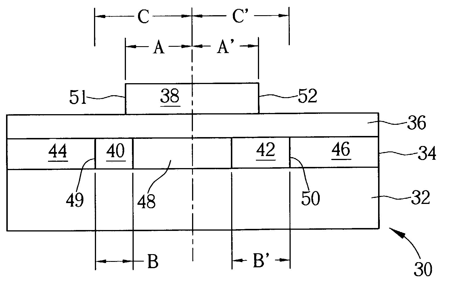
[0026]Please refer to FIG. 6 of a cross-sectional diagram of a thin-film transistor according to the present-invention. A thin-film transistor 30 shown in FIG. 6 is used as a pixel switch. However, the thin-film transistor 30 may also be used in other functional circuits in a liquid crystal display or in other electronic products. Normally, the thin-film transistor 30 is an n-type thin-film transistor. However, the thin-film transistor 30 may also be a p-type thin-film transistor according to the present invention.

[0027]The thin-film transistor 30 includes a semiconductor layer 34 positioned on a substrate 32, a gate insulating layer 36 positioned on the semiconductor layer 34, and a gate 38 positioned on the gate insulating layer 36. The semiconductor layer 34 includes two lightly doped drains 40 and 42 formed in different lengths, and two source / drain regions 44 and 46 adjacent to the gate 38. The lightly doped drains 40, 42 and the source / drain regions 44, 46 are all n-type doped...

fourth embodiment

[0037]Please refer to FIG. 13. FIG. 13 is a cross-sectional diagram of a bottom gate thin-film transistor according to the present invention. As shown in FIG. 13, the bottom gate thin-film transistor 100 includes a gate 104 positioned on a substrate 102, a gate insulating layer 106 positioned on the gate 104 and the substrate 102, and a semiconductor layer 108 positioned on the gate insulating layer 106. The semiconductor layer 108 includes a channel region 110, two lightly doped drains 112 and 114 having different lengths on both sides of the channel region 110, and two source / drain regions 116 and 118 respectively next to the lightly doped drains 112 and 114. The lightly doped drains 112, 114 and the source / drain regions 116, 118 are all n-type doped regions. The lengths of the lightly doped drains 112 and 114 range between 0 and 3.5 μm, respectively. The gate 104 is made of conductive materials such as metal or doped polysilicon. It is noteworthy that the bottom gate thin-film tr...


PUM


Abstract

An asymmetry thin-film transistor includes a substrate, a semiconductor layer and a gate positioned on the substrate. The semiconductor layer includes a first lightly doped region and a first heavily doped region adjacent to a first gate side, and a second lightly doped region together with a second heavily doped region adjacent to a second gate side. A first junction is between the first lightly doped region and the first heavily doped region. A second junction is between the second lightly doped region and the second heavily doped region. A distance between the first junction and the first gate side is unequal to a distance between the second junction and the second gate side.

Description

BACKGROUND OF INVENTION[0001]1. Field of the Invention[0002]The present invention relates to an asymmetry thin-film transistor (TFT), and more particularly, to an asymmetry thin-film transistor in a liquid crystal display.[0003]2. Description of the Prior Art[0004]From the fact that a thin-film transistor having an active layer formed of a crystalline silicon film on a substrate having an insulating surface has a high electric field effect mobility, it is possible to form a variety of functional circuits. For example, in the active matrix liquid crystal device (AMLCD) employing the crystalline silicon thin-film transistor, a thin-film transistor used as a pixel switch is formed in every pixel of an imaged is play region, and a thin-film transistor used in a drive circuit is formed in the periphery of the image display region.[0005]Since the functions and the operating conditions of the thin-film transistors in the pixel and the drive circuit are not the same, the characteristics tha...

Claims


Application Information

Patent Timeline
Patent Type & Authority Patents(United States)
IPC IPC(8): H01L29/04H01L21/336H01L29/786
CPCH01L29/78666H01L29/66742
Inventor CHEN, KUN-HONG
Owner AU OPTRONICS CORP
Features
  • Generate Ideas
  • Intellectual Property
  • Life Sciences
  • Materials
  • Tech Scout
  • Unparalleled Data Quality
  • Higher Quality Content
  • 60% Fewer Hallucinations
Learn More