Eureka AIR delivers breakthrough ideas for toughest innovation challenges, trusted by R&D personnel around the world.

Photodetector employing slab waveguide modes

a waveguide mode and waveguide technology, applied in the field of infrared radiation detection apparatus, can solve the problems of increasing the cost of hgcdte material, reducing the yield of hgcdte material, and relatively independent wavelength of iii–v mqw material, so as to achieve the effect of reducing cost, increasing yield and cos

Active Publication Date: 2006-11-21
LOCKHEED MARTIN CORP
View PDF8 Cites 2 Cited by
  • Summary
  • Abstract
  • Description
  • Claims
  • Application Information

AI Technical Summary

Benefits of technology

[0008]A third object of the invention is to provide an IR photodetector at a low cost. A photodetector that satisfies this third object is either of the above embodiments fabricated from III–V MQW material. III–V MQW material, such as that formed of AlGaAs / GaAs, is significantly less expensive than many other materials sensitive to IR radiation. Further, the cost of the III–V MQW material is relatively independent of the wavelength of the IR radiation to be absorbed. The cost of HgCdTe material increases significantly as the absorption IR wavelength increases. III–V MQW material is also available in substrate sizes significantly larger than HgCdTe further reducing costs. The cost of fabricating photodetectors from III–V MQW material is significantly less than other materials as well. A number of commercial devices are fabricated from III–V materials resulting in stable fabrication processes with very narrow tolerances, resulting in higher yields and lower costs.
[0009]A fourth object of the invention is to provide a multi-color IR photodetector design that does not compromise sensitivity relative to a single color IR photodetector. A photodetector that satisfies this fourth objective is the second of the above embodiments. As the position of the electric field maxima produced in the photodetector are due to creation of waveguide modes, the IR absorbing layers can be precisely located to minimize sensitivity loss. Sensitivity loss is further reduced by minimizing ohmic losses in the grating by placing the grating outside the high field region of the multi-color IR photodetector. That is, by locating the grating in the cladding layer where the electric field is low, ohmic losses are reduced, resulting in greater field strength for absorption by the two or more IR absorbing layers.

Problems solved by technology

Further, the cost of the III–V MQW material is relatively independent of the wavelength of the IR radiation to be absorbed.
The cost of HgCdTe material increases significantly as the absorption IR wavelength increases.
A number of commercial devices are fabricated from III–V materials resulting in stable fabrication processes with very narrow tolerances, resulting in higher yields and lower costs.

Method used


Image

  • Photodetector employing slab waveguide modes
  • Photodetector employing slab waveguide modes
  • Photodetector employing slab waveguide modes

Examples


first embodiment

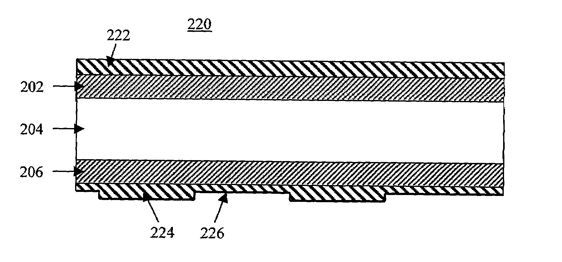
[0024]The present invention employs the TM modes described above to enhance the performance of IR photodetectors. The slab 200 for a slab waveguide photodetector according to the present invention is illustrated in FIG. 2A. The slab 200 includes an IR absorbing layer 204 and first and second contacts 202, 206 on either side of the IR absorbing layer 204. FIG. 2A includes a vector labeled EI that indicates the direction of the electric field of the incident IR radiation that is to be absorbed. A second vector, labeled EA, indicates the direction of the electric field required for strong absorption by the IR absorbing layer 204 if the IR absorbing layer 204 is formed of MQW material.

[0025]The IR absorbing layer 204 is preferably formed of any one of several MQW materials. Selection of the particular MQW material and design is determined by what wavelength of IR radiation is to be absorbed. A slab waveguide QWIP may operate in any of the three following wavelength ranges. The middle wa...

second embodiment

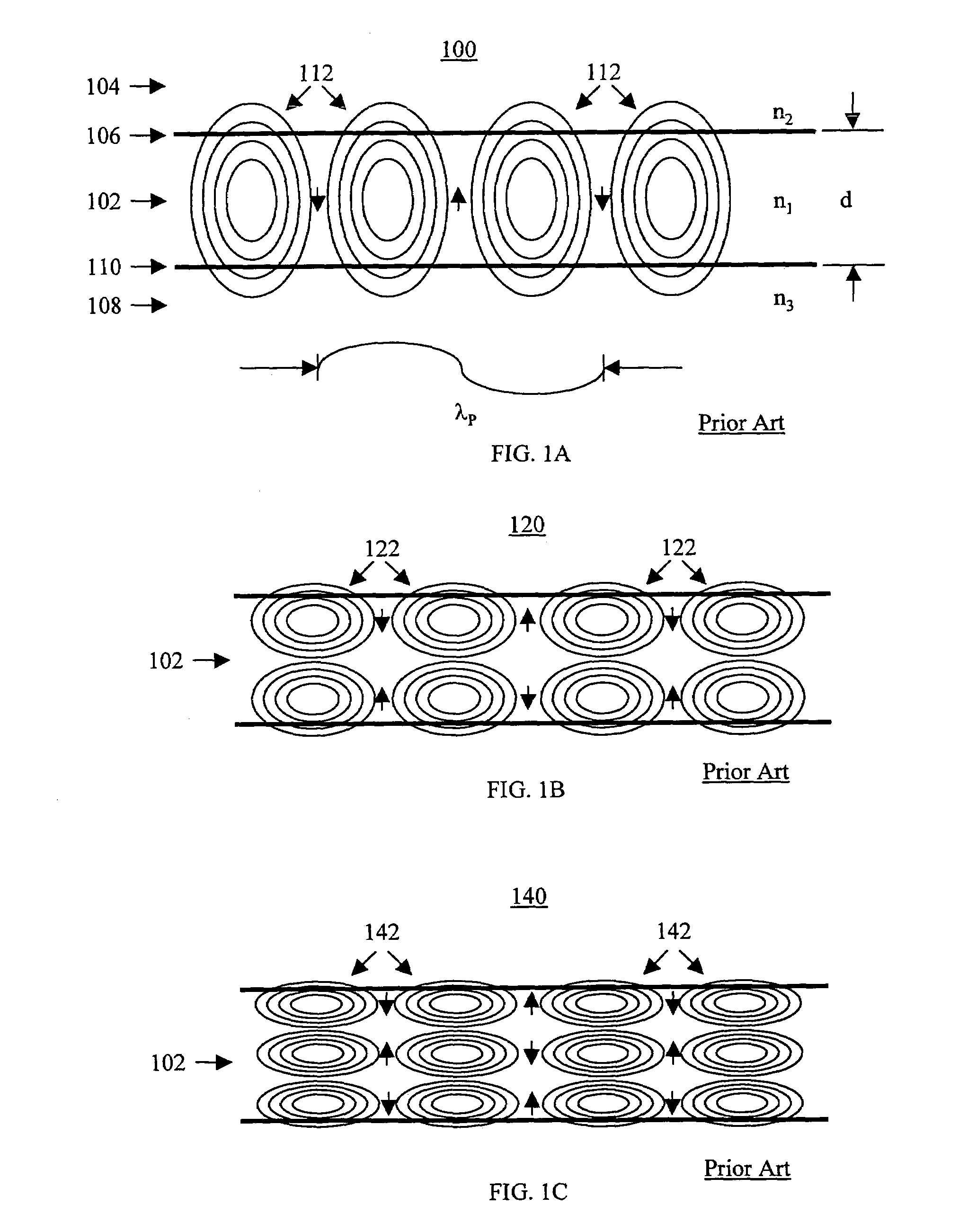
[0040]the present invention is based on the fact that the ideal dielectric slab waveguide structure 100 can support TM modes for radiation at different free space wavelengths. A multi-color slab waveguide QWIP 300 based upon different free space wavelengths is shown in FIG. 3A. The multi-color slab waveguide QWIP 300 includes first, second, and third contact layers 302, 304, 306 to allow detection of two different bands of IR radiation separately. A first band of IR radiation is absorbed in a first IR absorbing layer 308, while a second band of IR radiation is absorbed in a second IR absorbing layer 310. A preferred, though optional, antireflection coating 312 may be placed on the top surface of the multi-color slab waveguide QWIP 300. A cladding layer 314 is placed on the third contact 306. As with the slab waveguide QWIP 220, a reflective grating is formed on a surface of the cladding layer 314 to launch the IR radiation into the first and second IR absorbing layers 308, 310. The ...

third embodiment

[0050]A third embodiment, for multi-color sensitivity, employs a stack of independent slab waveguide QWIPs. A dual slab waveguide QWIP 600, illustrated in FIG. 6, includes a transmissive grating on a first cladding layer 602, a first contact 604, a first IR absorbing layer 606, a second contact 608, a mid-layer 610, a third contact 612, a second IR absorbing layer 614, a fourth contact 616, a second cladding layer 618 and a reflective layer 620. Each of these elements, except for the mid-layer 610, has generally been described above. For proper operation of the dual slab waveguide QWIP, the mid-layer 610 must have an index of refraction that is less than the indices of refraction of the first through fourth contacts 604, 608, 612, 616, and the first and second IR absorbing layers 606, 614. The result is that the first and second IR absorbing layers 606, 614 are located in independent slab waveguides as the two bands of IR radiation undergo TIR at the mid-layer 610.

[0051]In a preferr...


PUM


Abstract

A photodetector for detecting infrared radiation (IR) using a slab waveguide is described. The slab waveguide photodetector operates by resonating transverse magnetic or electric modes within the slab from the incident IR. An IR absorbing layer is located within the slab waveguide photodetector where the magnitude of the electric field vector is greatest. This permits the use of a thinner IR absorbing layer without sacrificing photoresponse. Multi-color slab waveguide photodetectors are permitted because multiple transverse magnetic or electric modes resonate within the slab waveguide. A reflective or transmissive grating is used to launch the IR into the IR absorbing layer through a cladding or antireflection layer.

Description

FIELD OF THE INVENTION[0001]The present invention relates to an apparatus for detecting radiation. In particular, the present invention provides for detecting infrared radiation using waveguide modes.BACKGROUND OF THE INVENTION[0002]Photodetectors for infrared (IR) radiation have many applications. IR radiation can often be used to detect objects where visible light is either blocked or not present. Thus, it is possible to use IR detection at night or through clouds, dust, or haze. An IR photodetector can be in the form of either a single detecting element or an array of such detecting elements to produce an image. A photodetector that produces such an image is termed a focal plane array.[0003]IR radiation can be detected by various methods. One such method is using a material that generates electric charge carriers in response to absorbing incident IR radiation. Examples of such photosensitive material are mercury cadmium telluride (HgCdTe) and a multi-layered structure termed a mu...

Claims


Application Information

Patent Timeline
Patent Type & Authority Patents(United States)
IPC IPC(8): G01J5/00
CPCB82Y20/00G01J1/42H01L31/0232H01L31/03046H01L31/035236H01L31/1035Y02E10/544H01L31/02327
Inventor BROUNS, AUSTIN J.
Owner LOCKHEED MARTIN CORP
Why Eureka
Eureka Blog
Learn More