Amplifier arrangement

a technology of amplifier arrangement and amplifier, applied in the direction of negative-feedback circuit arrangement, single-ended push-pull amplifier, gain control, etc., can solve the problems of unstable operation, higher power requirement, and unwanted parasitic pole point under different conditions, and achieve high conductance

Inactive Publication Date: 2006-11-28
INFINEON TECH AG
View PDF4 Cites 25 Cited by
  • Summary
  • Abstract
  • Description
  • Claims
  • Application Information

AI Technical Summary

Benefits of technology

[0009]The proposed amplifier arrangement makes it possible to overcome the stability problems by virtue of the controllable resistance in the coupling path of the output transistor being able to be used to perform pole point / zero point compensation, for example, if this is required on the basis of the amplifier's load and bias conditions. This means that it is possible to produce an operational amplifier with operating-point-dependent Miller frequency compensation which has a lower power consumption given the same stability.
[0014]In line with one exemplary implementation of the invention, the controllable resistance may additionally comprise a bias transistor whose controlled path is connected in parallel with the controllable resistance. The control input of the bias transistor may have a bias signal applied to it. This means that it is possible to retain the desired, comparatively high conductance of the total controllable resistance even for very large load currents through the output transistor.

Problems solved by technology

In such operational amplifiers, however, the problem may arise that unwanted parasitic pole points arise under different load and bias conditions.
However, this disadvantageously results in a higher power requirement.
However, stability problems may arise under different load conditions.
The stability problems arise particularly disadvantageously if the operational amplifier is in the form of a class AB operational amplifier.

Method used


Image

  • Amplifier arrangement
  • Amplifier arrangement
  • Amplifier arrangement

Examples


Embodiment Construction

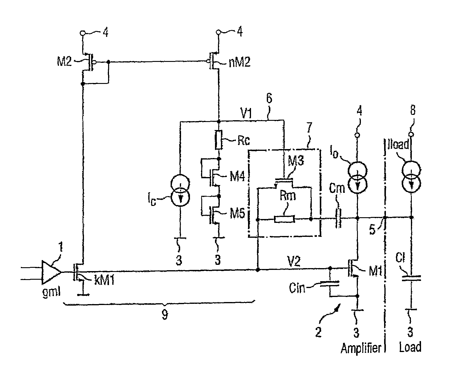
[0027]FIG. 1 shows a circuit diagram of an exemplary operational amplifier in accordance with the invention, comprising an input stage 1 and an output stage 2, which is connected downstream of the input stage. The output stage 2 has an output transistor M1 whose control connection, namely its gate connection, is connected to the output of the input stage 1. The controlled source / drain path of the output transistor M1 connects a current source I0 to a reference potential connection 3. A further connection on the current source I0 is connected to a supply potential connection 4. Between the current source I0 and the output transistor M1, the output 5 of the amplifier arrangement is formed. Between the gate connection and the source connection (on the reference potential side) of the output transistor M1, a parasitic gate / source capacitance Cin is shown. To compensate for frequency dependencies caused by the “Miller effect”, a Miller capacitance Cm is provided which is connected betwee...


PUM


Abstract

The invention provides an amplifier arrangement which is of multistage design. The output transistor in the output stage has a coupling path between its control input and its controlled path. The coupling path comprises a series circuit comprising a Miller compensation capacitance and a resistance with a controllable resistance value. It is thus possible to ensure stable operation of the amplifier regardless of bias and load conditions while simultaneously reducing the quiescent current drawn.

Description

REFERENCE TO RELATED APPLICATIONS[0001]This application claims the benefit of the priority date of German application DE 103 45 521.3, filed on Sep. 30, 2003, the contents of which are herein incorporated by reference in their entirety.FIELD OF INVENTION[0002]The present invention relates to an amplifier arrangement.BACKGROUND OF THE INVENTION[0003]An amplifier arrangement, more particularly an operational amplifier having Miller compensation is described, by way of example, in the printed document from Gregorian Roubik “Introduction to CMOS OP-AMPS and Comparators”, John Wiley and Sons, 1999, Chapter 4.4. In such operational amplifiers, however, the problem may arise that unwanted parasitic pole points arise under different load and bias conditions.[0004]If no pole point / zero point compensation is carried out for these pole points, the parasitic pole could be shifted to higher frequencies. However, this disadvantageously results in a higher power requirement. Otherwise, the stabili...

Claims


Application Information

Patent Timeline
Patent Type & Authority Patents(United States)
IPC IPC(8): H03F1/14H03F1/08H03F1/34H03F3/30H03F3/45
CPCH03F1/086H03F3/3022
Inventor KLEIN, AXELSCHLEDZ, RALF-RAINERAUGUSTYNIAK, MARCIN
Owner INFINEON TECH AG
Why Eureka
Try Eureka