Method of submicron metallization using electrochemical deposition of recesses including a first deposition at a first current density and a second deposition at an increased current density

a technology of electrochemical deposition and submicron metallization, which is applied in the direction of printed circuits, semiconductor devices, printed circuits, etc., can solve the problems of low current density plating waveforms that are often quite slow in producing metal films of the requisite thickness

Inactive Publication Date: 2006-12-05
SEMITOOL INC
View PDF242 Cites 9 Cited by
  • Summary
  • Abstract
  • Description
  • Claims
  • Application Information

AI Technical Summary

Benefits of technology

[0016]The present inventors have found that application of metallization, particularly copper metallization, using low current density plating waveforms provides better trench and via filling results when compared to high current density plating waveforms. This is particularly true when additive-free plating solutions are used. However, such low current density plating waveforms are often quite slow in producing metal films of the requisite thickness. Accordingly, a low current density plating waveform is used during initial plating operations while a high current density plating waveform is used to decrease the fill time and, if desired, provide a different film morphology, some time after the initial plating operations are complete.
[0017]In accordance with one embodiment of the present invention, the waveshape and its frequency are used to influence the surface morphology of the copper metallization deposit. Further, high metal concentrations in the additive-free plating solutions are used to provide more effective filling of the trench and via structures.
[0018]With respect to plating solutions that include additives, the present inventors have found that the plating process may be optimized by employing low metal concentration plating solutions. Such solutions produce higher quality filling of the trenches and vias when compared with copper metallization deposited using solutions having high metal concentrations.
[0019]Methods for depositing a metal into a micro-recessed structure in the surface of a microelectronic workpiece are disclosed. The methods are suitable for use in connection with additive free as well as additive containing electroplating solutions. In accordance with one embodiment, the method includes making contact between the surface of the microelectronic workpiece and an electroplating solution in an electroplating cell that includes a cathode formed by the surface of the microelectronic workpiece and an anode disposed in electrical contact with the electroplating solution. Next, an initial film of the metal is deposited into the micro-recessed structure using at least a first electroplating waveform having a first current density. The first current density of the first electroplating waveform is provide to enhance the deposition of the metal at a bottom of the micro-recessed structure. After the this initial plating, deposition of the metal is continued using at least a second electroplating waveform having a second current density. The second current density of the second electroplating waveform is provided to assist in reducing the time required to substantially complete filling of the micro-recessed structure.

Problems solved by technology

However, such low current density plating waveforms are often quite slow in producing metal films of the requisite thickness.

Method used


Image

  • Method of submicron metallization using electrochemical deposition of recesses including a first deposition at a first current density and a second deposition at an increased current density
  • Method of submicron metallization using electrochemical deposition of recesses including a first deposition at a first current density and a second deposition at an increased current density
  • Method of submicron metallization using electrochemical deposition of recesses including a first deposition at a first current density and a second deposition at an increased current density

Examples


Embodiment Construction

[0029]The present invention can be understood with reference to the experiments disclosed herein. Although the experiments were performed in connection with the plating of a metal comprising copper, it will be recognized that the teachings disclosed herein are so applicable to the electroplating of other metals. All the experiments were performed on 200 mm wafers using a plating tool, such as a plating tool available from Semitool, Inc., of Kalispell, Mont. Three plating baths were examined. The first one, bath 1 (either 24 g / L or 36 g / L copper) had no organic additives. The bath 2 (Additive A) and the bath 2 (Additive B) contain organic additives from different vendors.

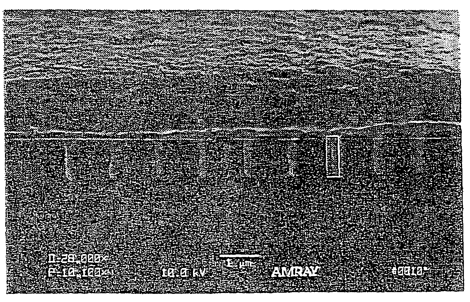
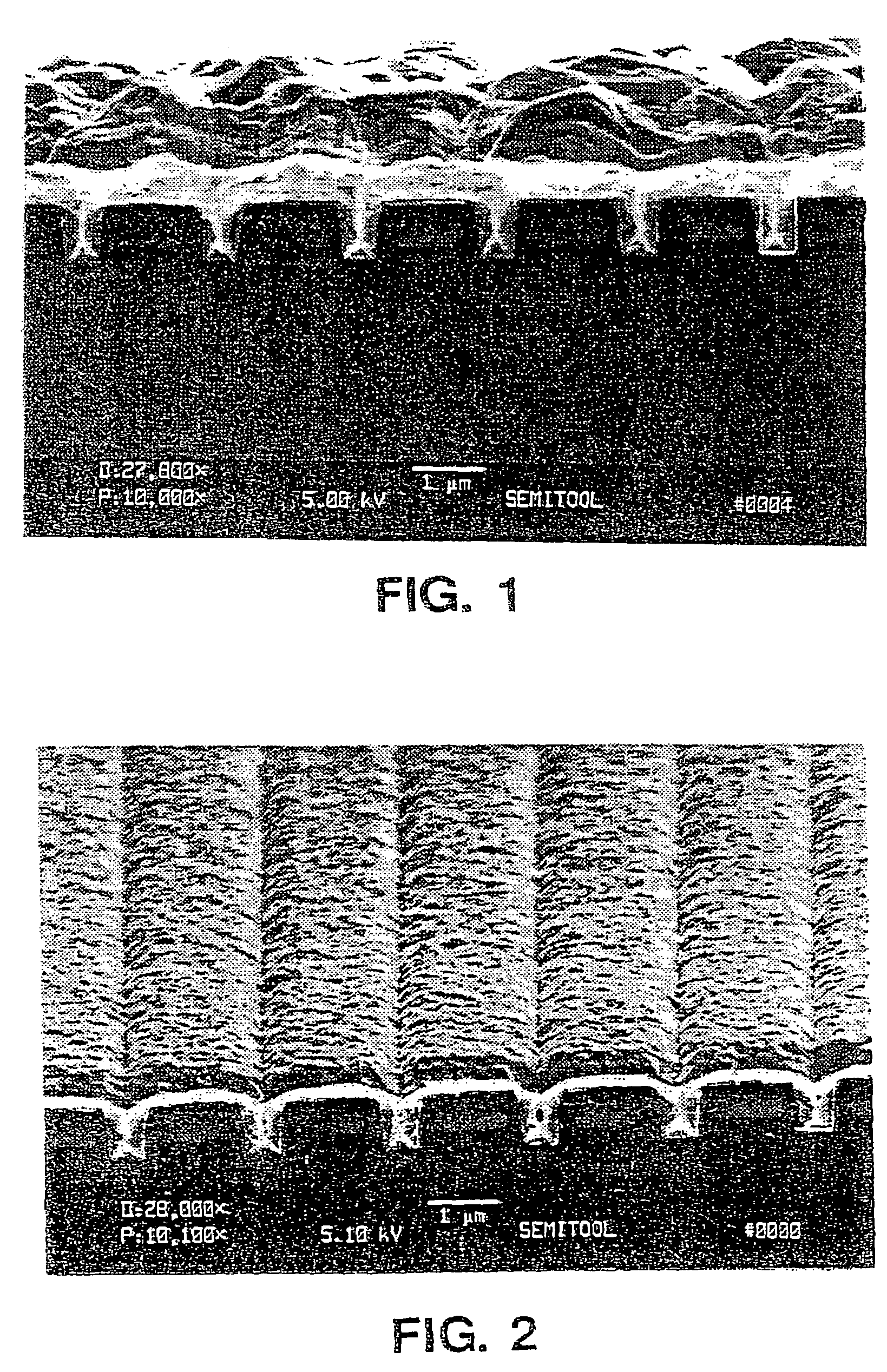
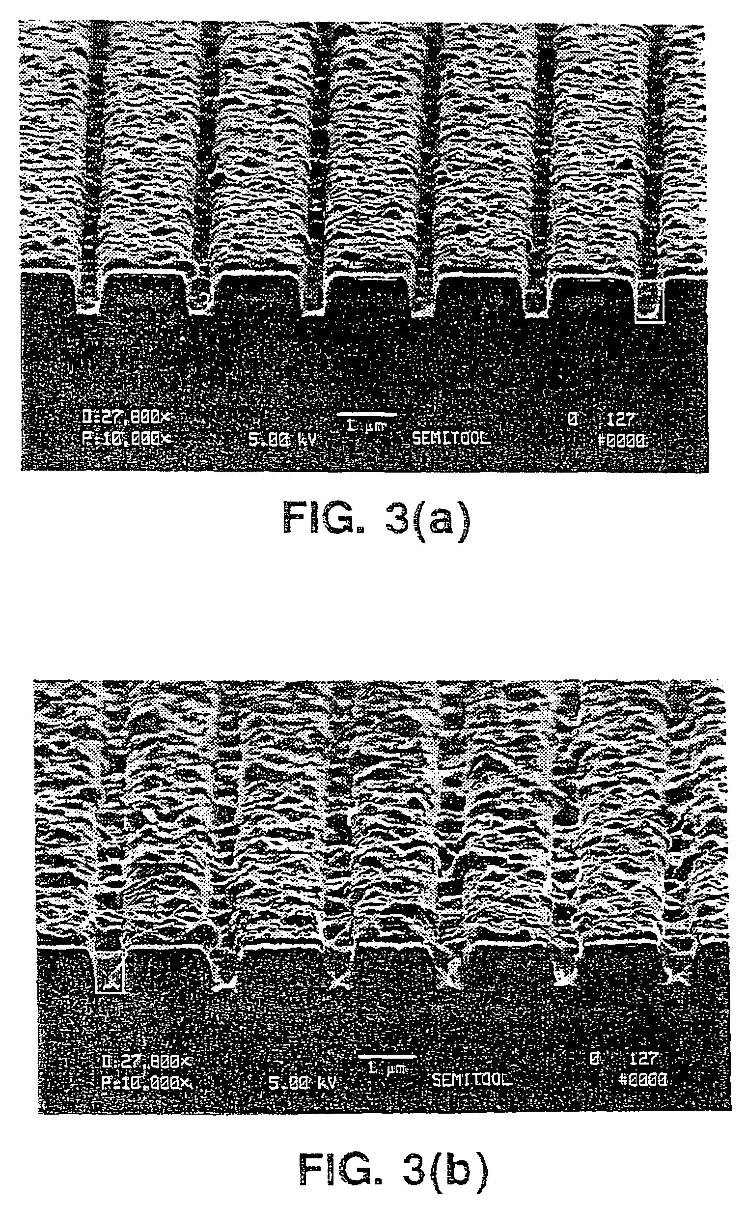
[0030]Good trench fill was obtained at low current density of 4 mA / cm2 for copper concentrations from 15 to 36 g / L. It is believed that the high micro-throwing power at low current density due to low concentration polarization is responsible for such trench fill at high copper concentrations. FIG. 1 presents a scanni...


PUM

PropertyMeasurementUnit
concentrationaaaaaaaaaa
diameteraaaaaaaaaa

Abstract

Methods for depositing a metal into a micro-recessed structure in the surface of a microelectronic workpiece are disclosed. The methods are suitable for use in connection with additive free as well as additive containing electroplating solutions. In accordance with one embodiment, the method includes making contact between the surface of the microelectronic workpiece and an electroplating solution in an electroplating cell that includes a cathode formed by the surface of the microelectronic workpiece and an anode disposed in electrical contact with the electroplating solution. Next, an initial film of the metal is deposited into the micro-recessed structure using at least a first electroplating waveform having a first current density. The first current density of the first electroplating waveform is provided to enhance the deposition of the metal at a bottom of the micro-recessed structure. After this initial plating, deposition of the metal is continued using at least a second electroplating waveform having a second current density. The second current density of the second electroplating waveform is provided to assist in reducing the time required to substantially complete filling of the micro-recessed structure.

Description

CROSS-REFERENCE TO RELATED APPLICATIONS[0001]This application is a continuation of U.S. application Ser. No. 09 / 815,931, filed Mar. 23, 2001 now U.S. Pat. No. 6,806,186 which is a continuation of International PCT Application No. PCT / US99 / 23187, filed Oct. 5, 1999, which claims the benefit of U.S. Provisional Patent Application No. 60 / 103,061, filed Oct. 5, 1998, and is also a continuation-in-part of U.S. patent application Ser. No. 09 / 018,783, filed Feb. 4, 1998.STATEMENT REGARDING FEDERALLY SPONSORED RESEARCH OR DEVELOPMENT[0002]Not ApplicableBACKGROUND OF THE INVENTION[0003]An integrated circuit is an interconnected ensemble of devices formed within a semiconductor material and within a dielectric material that overlies a surface of the semiconductor material. Devices which may be formed within the semiconductor material include MOS transistors, bipolar transistors, diodes and diffused resistors. Devices which may be formed within the dielectric include thin-film resistors and ca...

Claims


Application Information

Patent Timeline
Patent Type & Authority Patents(United States)
IPC IPC(8): H01L21/4763H01L21/44C25D5/02C25D5/10C25D5/18H01L21/288H01L21/768
CPCC25D5/02C25D5/10C25D5/18C25D5/50H01L21/2885H01L21/76877H01L21/76883C25D7/123C25D5/605C25D5/611
Inventor CHEN, LINLINGRAHAM, LYNDON W.RITZDORF, THOMAS L.FULTON, DAKINBATZ, JR., ROBERT W.
Owner SEMITOOL INC
Why Eureka
Try Eureka