Methods for intelligent caching in an embedded DRAM-DSP architecture

a technology of embedded dram and dsp, applied in the field of microsystem architecture, can solve the problems of limiting system performance in memory-intensive processing applications, prohibitively expensive srams of the same size, and slowing down the processor, so as to reduce the amount of instruction cache, and increase the number of rows

Inactive Publication Date: 2006-12-05
ROUND ROCK RES LLC
View PDF28 Cites 21 Cited by
  • Summary
  • Abstract
  • Description
  • Claims
  • Application Information

AI Technical Summary

Benefits of technology

[0011]The present invention solves these and other problems by providing an embedded-DRAM processor architecture with a program-controlled data transfer and caching structure that reduces or eliminates waiting time due to DRAM accessing. The present invention achieves this without the need for large SRAM caches as was required in prior art systems. The present invention incorporates an intelligent memory controller which performs prefetching and look-ahead operations to optimize the use of wide on-chip data paths available to the DRAM arrays. The present architecture is hardware efficient and involves parallel operations to accelerate the execution of standard programs. The present architecture is useful for reducing DRAM related delays in a wide variety of processor types, especially superscalar and VLIW processors with multiple pipelines.

Problems solved by technology

Larger but slower DRAMs are employed when a very large external memory is needed since fast SRAMs of the same size would be prohibitively expensive in most applications.
The use of a slower external DRAM often becomes the bottleneck that limits system performance in memory-intensive processing applications such as video compression and decompression.
Hence, current processor architectures need large amounts of on-chip SRAM to keep the memory system from creating a bottleneck and slowing down the processor.
A problem with the prior art is that SRAM takes on the order of 35 times more silicon area than DRAM for the same number of memory cells.
Also, when the data arrays to be manipulated do not fit on chip, extra data movement and less than optimal systems implementations are required to partition the problem.
This piecemeal approach requires extra overhead and system bus bandwidth.
Possibly more importantly, this piecemeal approach complicates programming, often leading to assembly coded implementations that increase the time-to-market and increase the development and maintenance costs of the system.
While prior art memory hierarchy concepts serve well in processors, such concepts may not be the best approaches for embedded-DRAM processor architectures.
First of all, large SRAM caches take up a significant amount of silicon area, largely defeating the purpose of integrating DRAM on to the processor.
When the processor executes image and signal processing algorithms, data caches become much less useful because image and signal data structures do not typically fit in the cache.
In fact, overall performance will often be degraded due to overhead associated with ineffective caching.
A problem that exists in prior art systems, especially DSPs and media processors, is the difficulty for compilers to efficiently translate a high-level language program into an efficient implementation.
The difficulty arises largely due to the complicated pointer manipulations and indexing needed to keep the pipelines of the architecture running near their peak efficiency.
When data caches are also included, the problem can be even more severe.
Thus, a problem with prior art DSPs and processors that employ data caching structures is the difficulty compilers have in generating efficient code due to their need to design very complicated pointer manipulation strategies and the need to account for second order cache side-effects.

Method used


Image

  • Methods for intelligent caching in an embedded DRAM-DSP architecture
  • Methods for intelligent caching in an embedded DRAM-DSP architecture
  • Methods for intelligent caching in an embedded DRAM-DSP architecture

Examples


Embodiment Construction

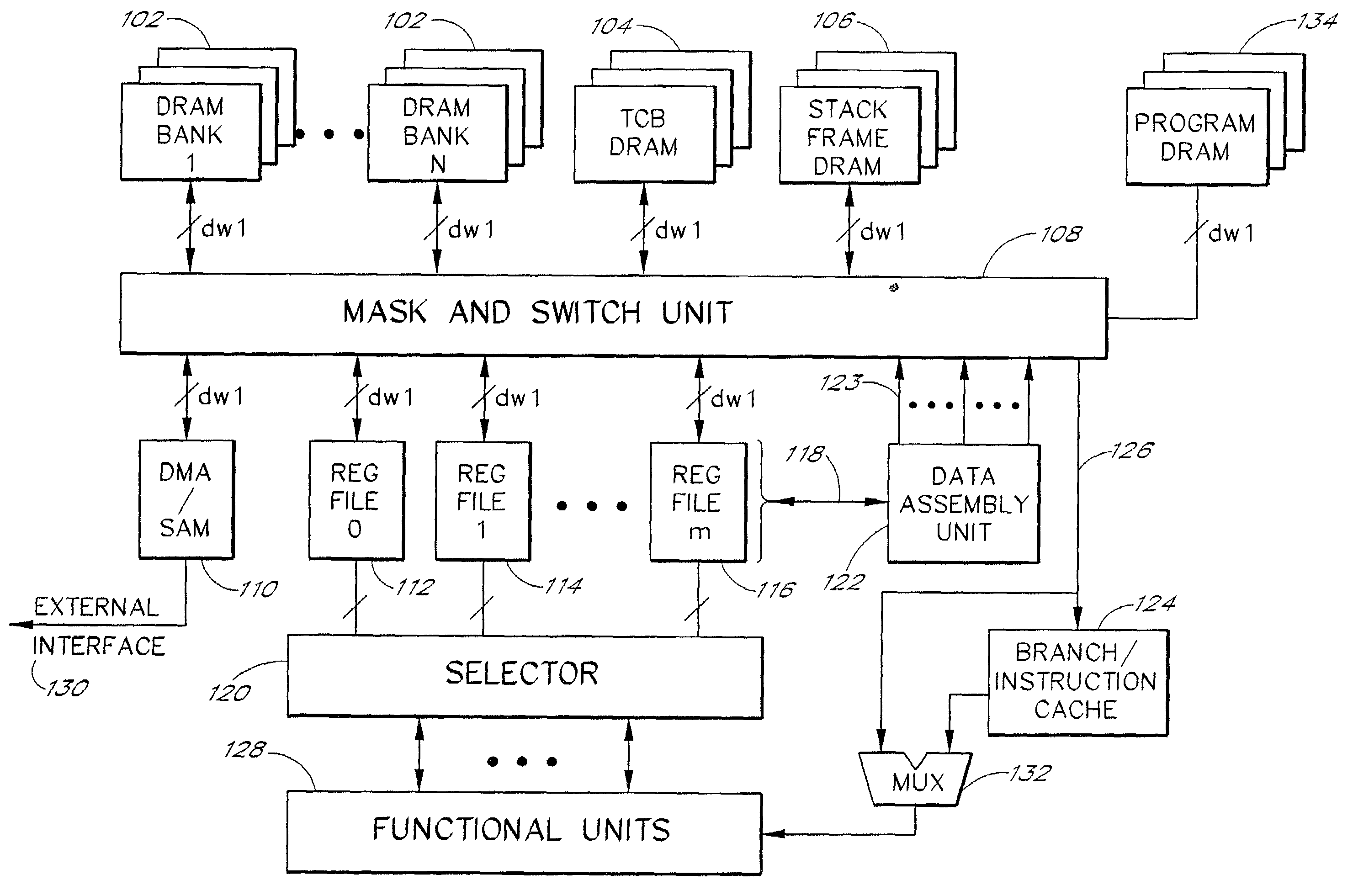
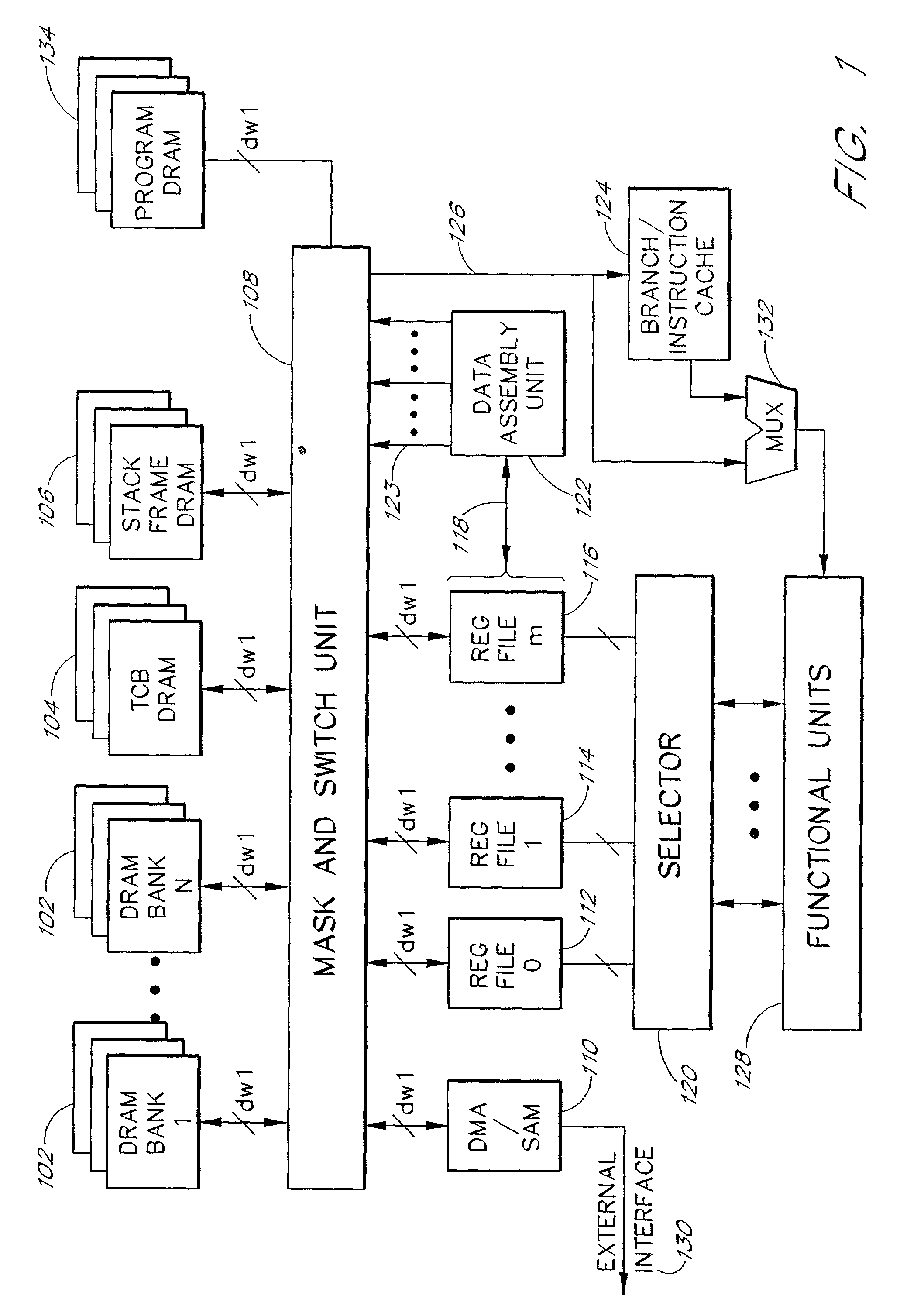
[0047]FIG. 1 is a block diagram that illustrates an embodiment of the embedded-DRAM processor architecture of the present invention. A set of N DRAM banks 102 are coupled to a mask and switch unit 108 via data busses of width dw1. The number dw1 is defined in words, and each word contains b bits. In the preferred embodiment, the number dw1 is equal to the number of columns in a DRAM row, for example, dw1=128. The DRAM banks 102 are preferably stacked according to the number of bits, b, in a word as defined by the architecture. For example, if a set of functional units 128 operate on 16-bit quantities, then b=16 and each of the DRAM array 102 is preferably stacked to provide dw1 16-bit words. For example, in the preferred embodiment, the number N is equal to 64, and each DRAM array 102 is organized as a stack of sixteen 16,384-bit DRAMs containing 128 columns and 128 rows. When stacked into 16-bit word modules, a total of 16 megabits are provided among all the DRAM arrays 102. Arrays...


PUM


Abstract

An efficient embedded-DRAM processor architecture and associated methods. In one exemplary embodiment, the architecture includes a DRAM array, a set of register files, set of functional units, and a data assembly unit. The data assembly unit includes a set of row-address registers and is responsive to commands to activate and deactivate DRAM rows and to control the movement of data throughout the system. A pipelined data assembly approach allowing the functional units to perform register-to-register operations, and allowing the data assembly unit to perform all load / store operations using wide data busses. Data masking and switching hardware allows individual data words or groups of words to be transferred between the registers and memory. Other aspects of the invention include a memory and logic structure and an associated method to extract data blocks from memory to accelerate, for example, operations related to image compression and decompression.

Description

REFERENCE TO RELATED APPLICATIONS[0001]This application is a divisional of U.S. patent application Ser. No. 10 / 001,007 filed Nov. 14, 2001, entitled “Embedded-DRAM-DSP Architecture,” which claims priority benefit of U.S. patent application Ser. No. 09 / 021,933 filed Feb. 11, 1998 of the same title, which claims priority benefit of U.S. provisional application Ser. No. 60 / 054,439 filed Aug. 1, 1997 of the same title.BACKGROUND OF THE INVENTION[0002]1. Field of the Invention[0003]This invention relates to the field of microsystems architectures. More particularly, the invention relates to memory access, memory hierarchy and memory control strategies targeted for use in embedded-DRAM (dynamic random access memory) digital signal processors (DSPs) and media processors.[0004]2. Description of the Related Art[0005]Digital signal processors (DSPs) are microprocessors optimized to execute multiply-accumulate intensive code on arrays of data. Media processors are similar to DSPs, but are furt...

Claims


Application Information

Patent Timeline
Patent Type & Authority Patents(United States)
IPC IPC(8): G06F15/00G06F9/30G06F9/40G06F9/38G06F12/08G06F15/78
CPCG06F9/30032G06F9/3012G06F9/30138G06F9/30141G06F9/3802G06F9/3804G06F15/7821G06F9/383G06F9/3842G06F9/3851G06F12/0862G06F9/3814G06F2212/6022
Inventor DOWLING, ERIC M.
Owner ROUND ROCK RES LLC
Why Eureka
Try Eureka