Microfabricated diamond element and method of fabricating microfabricated diamond element

Inactive Publication Date: 2006-12-12
SUMITOMO ELECTRIC IND LTD +1
View PDF2 Cites 10 Cited by
  • Summary
  • Abstract
  • Description
  • Claims
  • Application Information

AI Technical Summary

Benefits of technology

[0062]Since the de Broglie wave of electrons (or holes) traveling in the long-side direction and in the short-side direction forms a standing wave, electrons in the diamond become likely to be excited. The effec

Problems solved by technology

However, the luminous efficiencies were insufficient with the microfabr

Method used


Image

  • Microfabricated diamond element and method of fabricating microfabricated diamond element
  • Microfabricated diamond element and method of fabricating microfabricated diamond element
  • Microfabricated diamond element and method of fabricating microfabricated diamond element

Examples


first embodiment

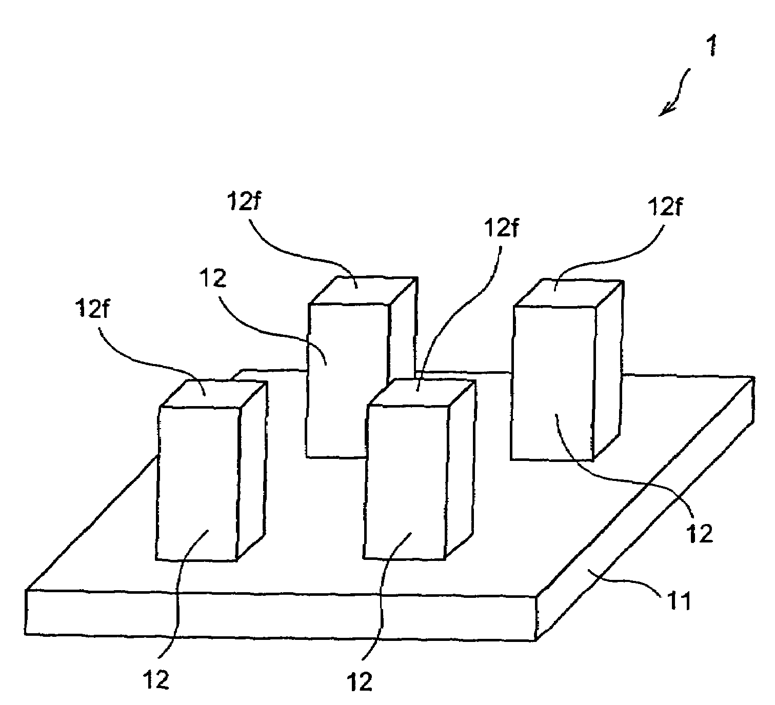
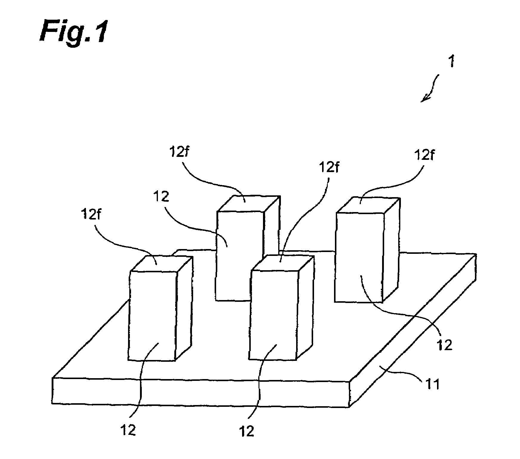
[0084]First, the structure of the microfabricated diamond element (diamond element 1) in the first embodiment will be described. FIG. 1 is a schematic diagram showing a simplified form of diamond element 1. The diamond element 1 is comprised of a substrate 11, and a plurality of quadrangular columns 12 (microscopic projections) arranged at equal intervals on the substrate 11, made of diamond, and having side faces of flat faces. The diamond making the quadrangular columns 12 demonstrates luminescence characteristics against excitation means such as electron beam irradiation, X-ray irradiation, photoexcitation, current injection, heating, or the like and has a broad or sharp overall spectrum of generated light, which has a particularly high luminous intensity at a certain wavelength. In this specification, this wavelength is referred to as an “emission peak wavelength λ [nm]”.

[0085]It is also conceivable to design the sectional shape of the columnar bodies (quadrangular columns 12) i...

second embodiment

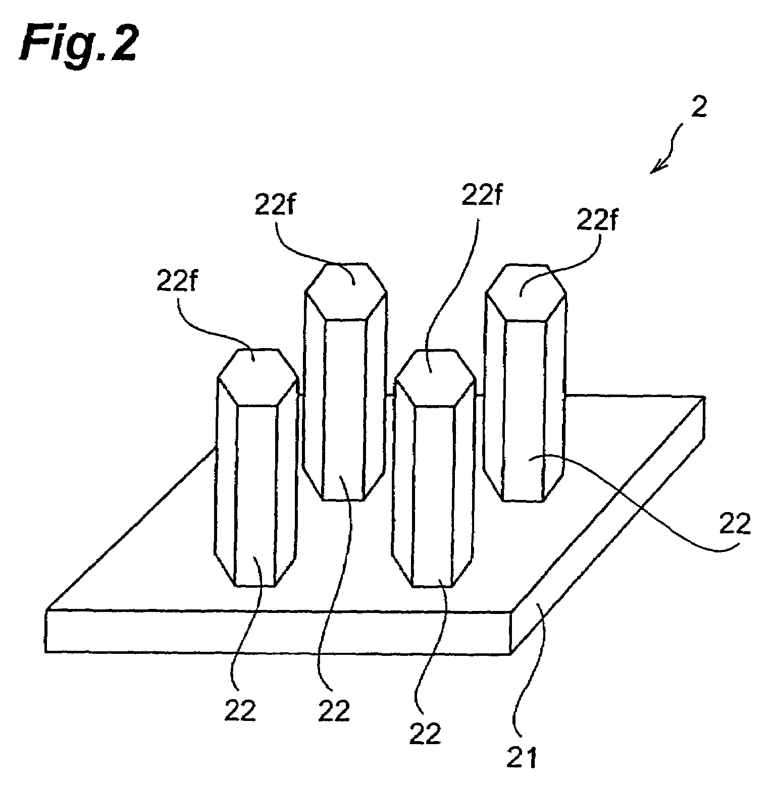
[0103]First, the structure of the microfabricated diamond element (diamond element 2) in the second embodiment will be described. FIG. 2 is a schematic diagram showing a simplified form of diamond element 2. The diamond element 2 is comprised of a substrate 21, and a plurality of hexagonal columns 22 (microscopic projections) arranged at equal intervals on the substrate 21, made of diamond, and having side faces of flat faces. The diamond making the hexagonal columns 22 demonstrates luminescence characteristics against excitation means such as electron beam irradiation, X-ray irradiation, photoexcitation, current injection, heating, or the like and has a broad or sharp overall spectrum of generated light, which has a particularly high luminous intensity at a certain wavelength (emission peak wavelength λ [nm]).

[0104]It is also conceivable to design the sectional shape of the columnar bodies (hexagonal columns 22) in agreement with another wavelength component instead of the emission...

third embodiment

[0112]First, the structure of the microfabricated diamond element (diamond element 3) in the third embodiment will be described. FIG. 3 is a schematic diagram showing a simplified form of diamond element 3. The diamond element 3 is comprised of a substrate 31, and a plurality of circular columns 32 (microscopic projections) arranged at equal intervals on the substrate 31 and made of diamond. The diamond making the circular columns 32 demonstrates luminescence characteristics against excitation means such as electron beam irradiation, X-ray irradiation, photoexcitation, current injection, heating, or the like and has a broad or sharp overall spectrum of generated light, which has a particularly high luminous intensity at a certain wavelength (emission peak wavelength λ [nm]).

[0113]It is also conceivable to design the sectional shape of the columnar bodies (circular columns 32) in agreement with another wavelength component instead of the emission peak wavelength, and to extract light...


PUM


Abstract

A diamond electron emission element is provided with a substrate, and a plurality of quadrangular columns (microscopic projections) composed of diamond and with side faces of flat faces, which are arranged at equal intervals on the substrate. A top end face (horizontal section) is of a quadrangular shape having a length of long sides being a [nm] and a length of short sides being ka [nm], and a thin film of SiO2 is formed on a side face on the short-edge side. The length a [nm] of long sides and the length ka [nm] of short sides satisfy relational expressions of Formulae (1) and (2) below.
C1=2a√{square root over (1+k2)}  (1)
nλ=C1  (2)
  • C1: a distance [nm] of a lap in a situation where light generated inside each quadrangular column goes around on a specific circuit while being reflected on the side faces of the quadrangular column,
  • n: an arbitrary positive integer, and
  • λ: an emission peak wavelength λ [nm] of the diamond making the quadrangular columns.

Description

BACKGROUND OF THE INVENTION[0001]1. Field of the Invention[0002]The present invention relates to microfabricated diamond elements used in light emitting devices and others, and methods of fabricating microfabricated diamond elements.[0003]2. Related Background Art[0004]The microfabricated diamond elements used in the conventional light emitting devices was those with PN junctions in diamond columns of arbitrary shape, for example, as described in New Diamond (Japan New diamond Forum) Vol. 17, No. 4 (2001), p10 and subsequent pages (Document 2).[0005]Other documents listed below also disclose the techniques related to the present invention.[0006][Document 1] Japanese Patent Application Laid-Open No. 2002-075171[0007][Document 2] New Diamond (Japan New Diamond Forum) Vol. 17 No. 4 (2001) p10 and subsequent pages[0008][Document 3] Extended Abstracts (The 47th Spring Meeting); The Japan Society of Applied Physics and Related Societies, No. 1 30a-YQ-3 (p377)[0009][Document 4] Extended Ab...

Claims


Application Information

Patent Timeline
IPC IPC(8): H01L33/00B82B1/00B82B3/00H01J1/304H01L33/16H01L33/34
CPCH01L33/20H01L33/34Y10T428/30H01J1/304
Inventor NISHIBAYASHI, YOSHIKIANDO, YUTAKAIMAI, TAKAHIRO
Owner SUMITOMO ELECTRIC IND LTD
Why Eureka
Try Eureka