Mask forming and removing method, and semiconductor device, an electric circuit, a display module, a color filter and an emissive device manufactured by the same method

a technology of emissive devices and masks, which is applied in the direction of semiconductor devices, electrical equipment, basic electric elements, etc., can solve the problems of undesirable etching and consuming vacuum processing equipment consumes a considerable amount of energy, etc., and achieves the effect of reducing manufacturing costs, reducing the number of steps, and facilitating lyophilic surface treatmen

Inactive Publication Date: 2006-12-12
SEIKO EPSON CORP
View PDF13 Cites 8 Cited by
  • Summary
  • Abstract
  • Description
  • Claims
  • Application Information

AI Technical Summary

Benefits of technology

[0015]Moreover, the present invention provides a method of forming a mask capable of enhancing adhesiveness of a member to be processed. The present invention is also intended to provide a method of forming a mask capable of enhancing patterning performance of the mask, as well as pattern forming performance of a material for patterning.
[0077]Further, an emissive device of the present invention is manufactured by any one of the above mask forming methods and / or by any one of the mask removing methods. Consequently, it is possible to manufacture the emissive device with the above-mentioned effects.

Problems solved by technology

However, the above manufacturing process and a semiconductor device manufactured by the process cause the following problems.
The vacuum-processing equipment consumes a considerable amount of energy including energy for fundamental units to process surrounding exhaust air and cooling water, when performing the vacuum process.
However, this etching undesirably consumes a considerable amount of energy.

Method used


Image

  • Mask forming and removing method, and semiconductor device, an electric circuit, a display module, a color filter and an emissive device manufactured by the same method
  • Mask forming and removing method, and semiconductor device, an electric circuit, a display module, a color filter and an emissive device manufactured by the same method
  • Mask forming and removing method, and semiconductor device, an electric circuit, a display module, a color filter and an emissive device manufactured by the same method

Examples


example 1

First Exemplary Embodiment

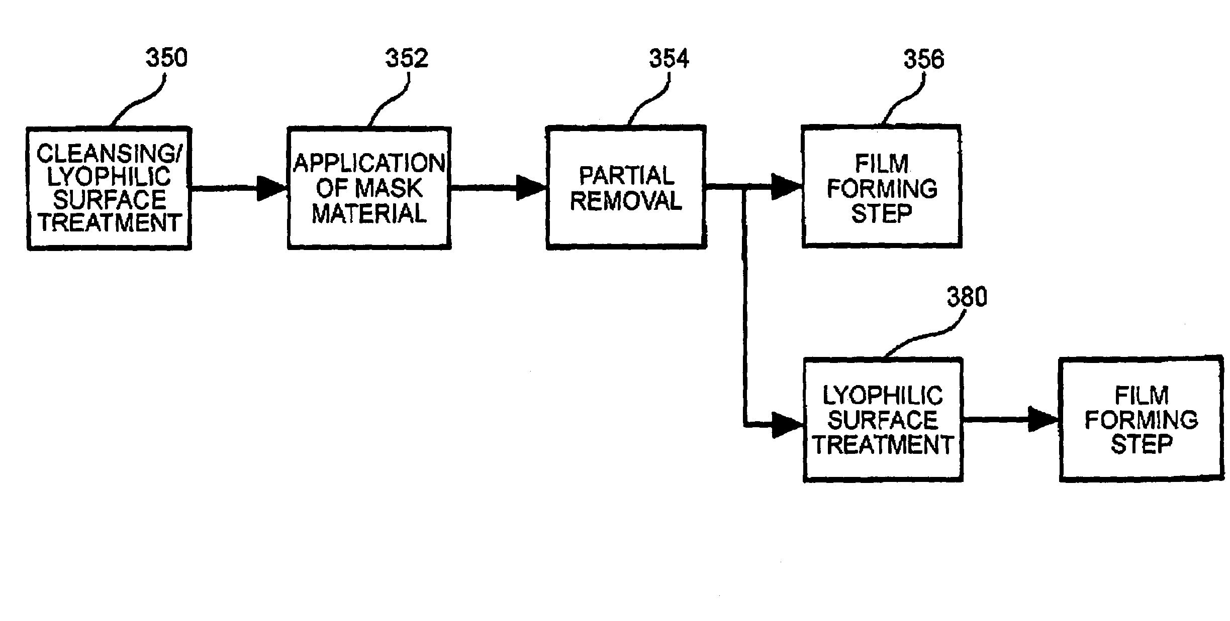
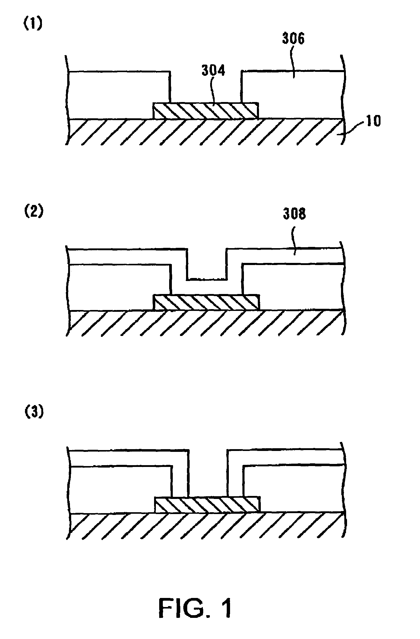
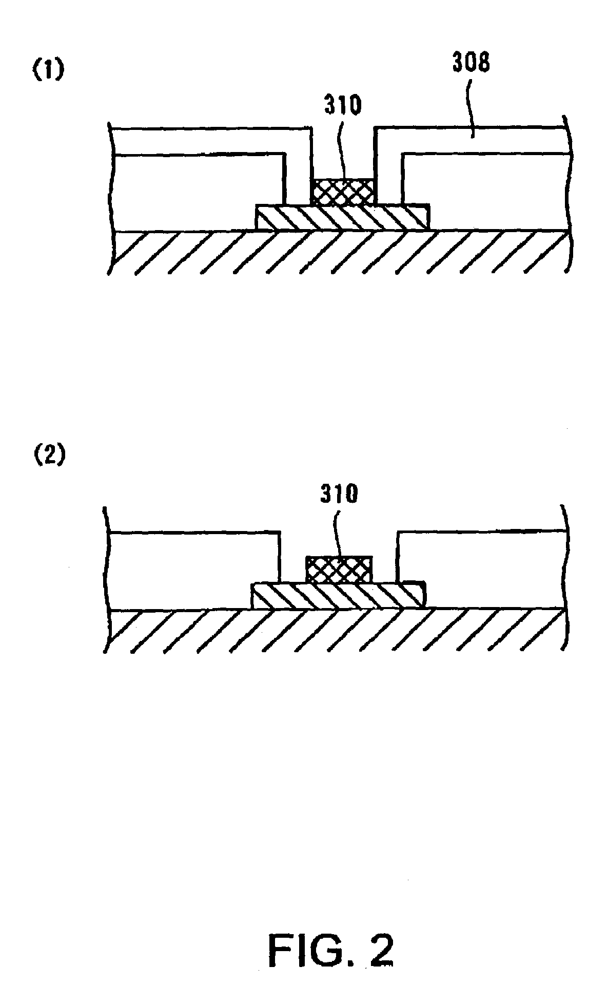
[0095]First, a mask forming method is explained as a first exemplary embodiment. The mask forming method according to the first exemplary embodiment performs patterning by conducting electric current to a metal pattern 304 in electrolytic solution and then electrolyzing a mask-material layer on the metal pattern 304 to remove it. The patterning forms a new pattern 310, shown in FIG. 2(b) on the metal pattern 304, which is formed on the surface of a member to be processed 10 shown in FIG. 1(a). The method includes first, forming the mask-material layer over the entire surface of the member to be processed, second, heating the mask-material layer, third, patterning by removing the mask-material layer that remains in a pattern-formation area in the electrolytic solution and fourth, heating the mask-material layer. Here, the member to be processed in the first exemplary embodiment may be a silicon wafer.

[0096]The mask forming method is first explained by taking...

second exemplary embodiment

[0110]Next, mask removing step according to the second exemplary embodiment is implemented by irradiating the polymerized film with ultraviolet rays. The member to be processed 10 is placed in a processing chamber 432 of a surface-reforming device 430 shown in FIG. 6, and an ultraviolet lamp 440 is placed above the processing chamber 432. The ultraviolet lamp 440 is placed inside an ultraviolet lamp chamber 442, where nitrogen gas can be replaceable, because it would be burned when lighted in the atmospheric air. The wall surface of the ultraviolet lamp chamber 442 on the side of the processing chamber 432 is formed of a glass plate 441 that transmits ultraviolet rays, such that the member to be processed 10 can be irradiated with ultraviolet rays. On the other hand, the wall surface of the processing chamber 432 on the side of the ultraviolet lamp chamber 442 is formed of a fluorite 431 that transmits ultraviolet rays. This configuration allows the member to be processed to be irra...

example 2

[0122]As the second example, FIGS. 9(a)–9(f) through FIGS. 11(a)–11(e) simply illustrate one example of a process of forming a thin film of organic electroluminescence (EL) used as an emissive layer of an emissive element. This process includes forming an electrode 607 located opposite a transparent conductive member 601, formed on a glass substrate 600 and sandwiching an emissive member 605.

[0123]First, the transparent conductive member 601 is deposited on the entire surface of the glass substrate 600 and etched to form a desired pattern as shown in FIG. 9(a) to FIG. 9(c).

[0124]Preferably, the glass substrate 600 is cleansed with a wet-type or a dry-type method as explained in the first example.

[0125]Moreover, the pattern is formed by etching after the transparent conductive member 601 is formed on the entire surface in this example. On the other hand, it may be also possible to employ a method of implementing the lyophobic surface treatment on the substrate excluding the pattern-f...


PUM

PropertyMeasurementUnit
temperatureaaaaaaaaaa
thicknessaaaaaaaaaa

Abstract

A mask forming method that can reduce manufacturing cost is disclosed. The method forms a mask on the surface of a member to be processed in order to form a desired pattern using liquid material for patterning. The method also includes applying resist to the entire surface of the member to be processed, drying the applied resist, patterning by removing the resist in a pattern-formation area using photolithography, and heating the resist.

Description

BACKGROUND OF THE INVENTION[0001]1. Field of Invention[0002]The present invention relates to manufacturing fields of semiconductor devices, liquid crystal devices and other elemental devices including stacked thin film layers. The present invention also relates to fields of high-density packages and more to a mask forming method to form a pattern using liquid material for patterning in the vicinity of atmospheric pressure, without requiring a reduced-pressure environment when manufacturing devices. Moreover, the present invention relates to a semiconductor device manufactured by the mask forming method.[0003]2. Description of Related Art[0004]In the related art, a wiring pattern is formed over elements, after the elements are formed on the surface of a wafer substrate, in manufacturing a semiconductor device.[0005]FIG. 15 and FIG. 16 show a process of related art patterning. When wiring is formed, for example, on the surface of a semiconductor wafer 1 shown in FIG. 15(a), a wiring l...

Claims


Application Information

Patent Timeline
Patent Type & Authority Patents(United States)
IPC IPC(8): H01L21/302C25D5/02C25D7/12H01L21/027H01L21/288H01L21/311H01L21/312H01L21/768
CPCC25D7/12H01L21/0272H01L21/76838H01L21/288H01L21/31127H01L21/31133H01L21/0274C25D5/022H01L21/32
Inventor MORI, YOSHIAKIMIYAKAWA, TAKUYASATO, MITSURUASUKE, SHINTAROTAKAGI, KENICHI
Owner SEIKO EPSON CORP
Why Eureka
Try Eureka