Discrete electronic component arrangement including anchoring, thermally conductive pad

a technology of electronic components and thermally conductive pads, which is applied in the direction of sustainable manufacturing/processing, final product manufacturing, casings/cabinets/drawer details, etc., can solve the problems of component terminal cracking, premature failure of components, oxidation and intergranular corrosion, etc., to reduce component thermal expansion, reduce component temperature and thermal expansion, and reduce fatigue

Active Publication Date: 2006-12-12
DELPHI TECH IP LTD
View PDF18 Cites 50 Cited by
  • Summary
  • Abstract
  • Description
  • Claims
  • Application Information

AI Technical Summary

Benefits of technology

[0008]An advantage of the present invention is that heat is carried away from the body of the electronic component, thereby reducing both the temperature of the component and its thermal expansion. Thus, the solder joints at the terminals of the component are subject to less fatigue.
[0009]Another advantage is that the thermally conductive element anchors the body of the electronic component to the substrate, thus limiting the amount of component thermal expansion that the solder joints must withstand and be subjected to.
[0010]Yet another advantage is that the thermally conductive element provides structural support to the electronic component and spaces the electronic component a certain distance away from the substrate. Thus, the thickness of the layers of solder between the terminals of the electronic component and the solder pads supported by the substrate may be greater, which may result in the solder joints having an increased life.

Problems solved by technology

The high power density requirements may result in premature failure of the components due to heat stress and thermal expansion.
For example, repeated thermal expansion may cause cracking in the solder joints at the terminals of the components, as well as oxidation and intergranular corrosion.
A typical power rating of a ceramic resistor chip, such as a model 2512 chip, is less than or equal to one watt per chip from room temperature up to 70° C. However, above 70° C. the power rating steadily falls to 0 watt at about 155° C. Temperature cycling testing reveals that such chips cannot pass a test including 1000 cycles between −40° C. aid 150° C. Many automotive applications require a high power chip to operate at an application temperature range of 85° C. to 105° C., which the chips are not able to reliably withstand.
However, this adds to the component cost and negates the advantage of surface mounted devices, which is in occupying as little space as possible.

Method used


Image

  • Discrete electronic component arrangement including anchoring, thermally conductive pad
  • Discrete electronic component arrangement including anchoring, thermally conductive pad

Examples


Embodiment Construction

[0013]The embodiments discussed below are not intended to be exhaustive or limit the invention to the precise forms disclosed in the following detailed description. Rather, the embodiments are chosen and described so that others skilled in the art may utilize their teachings.

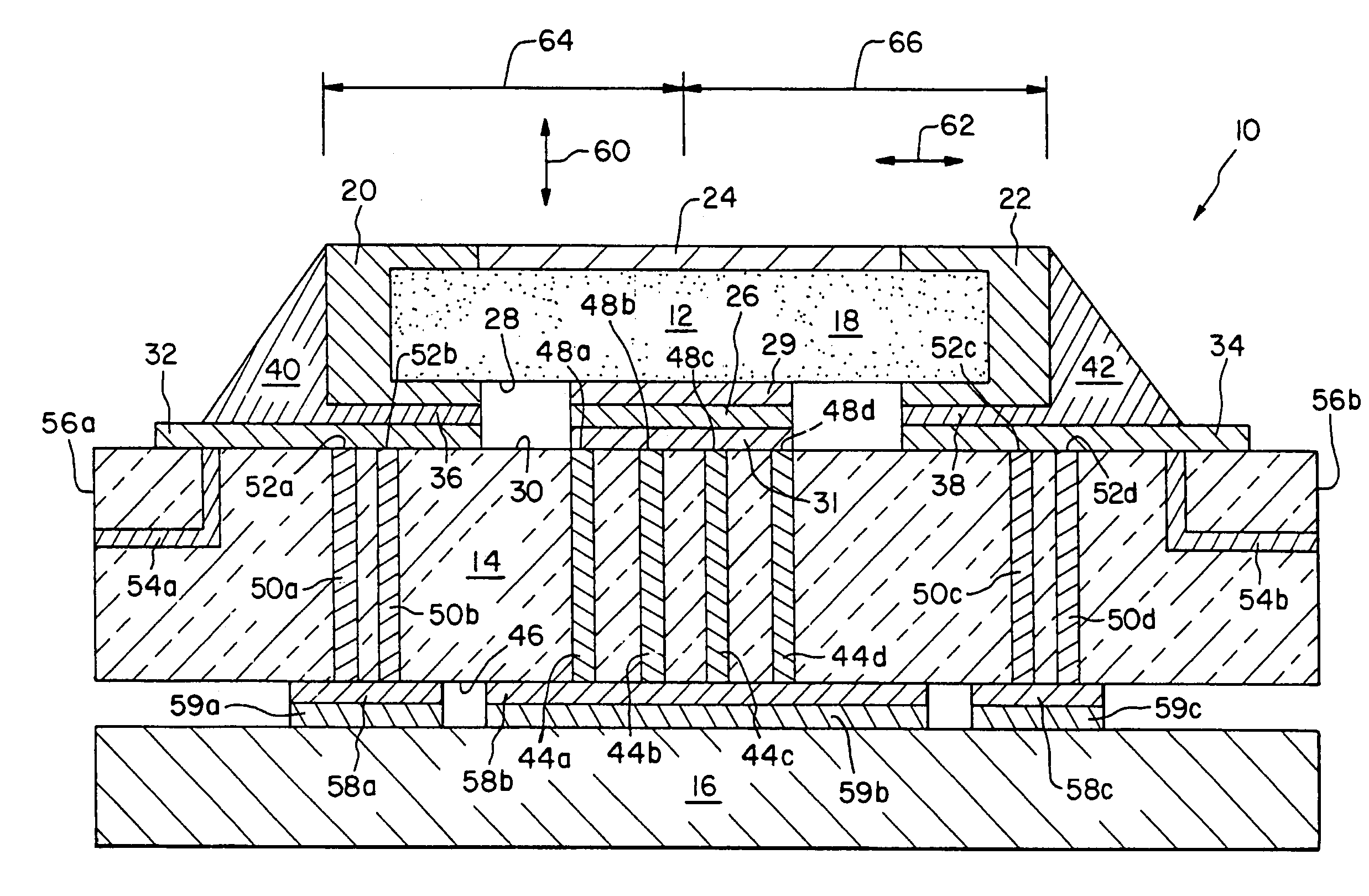
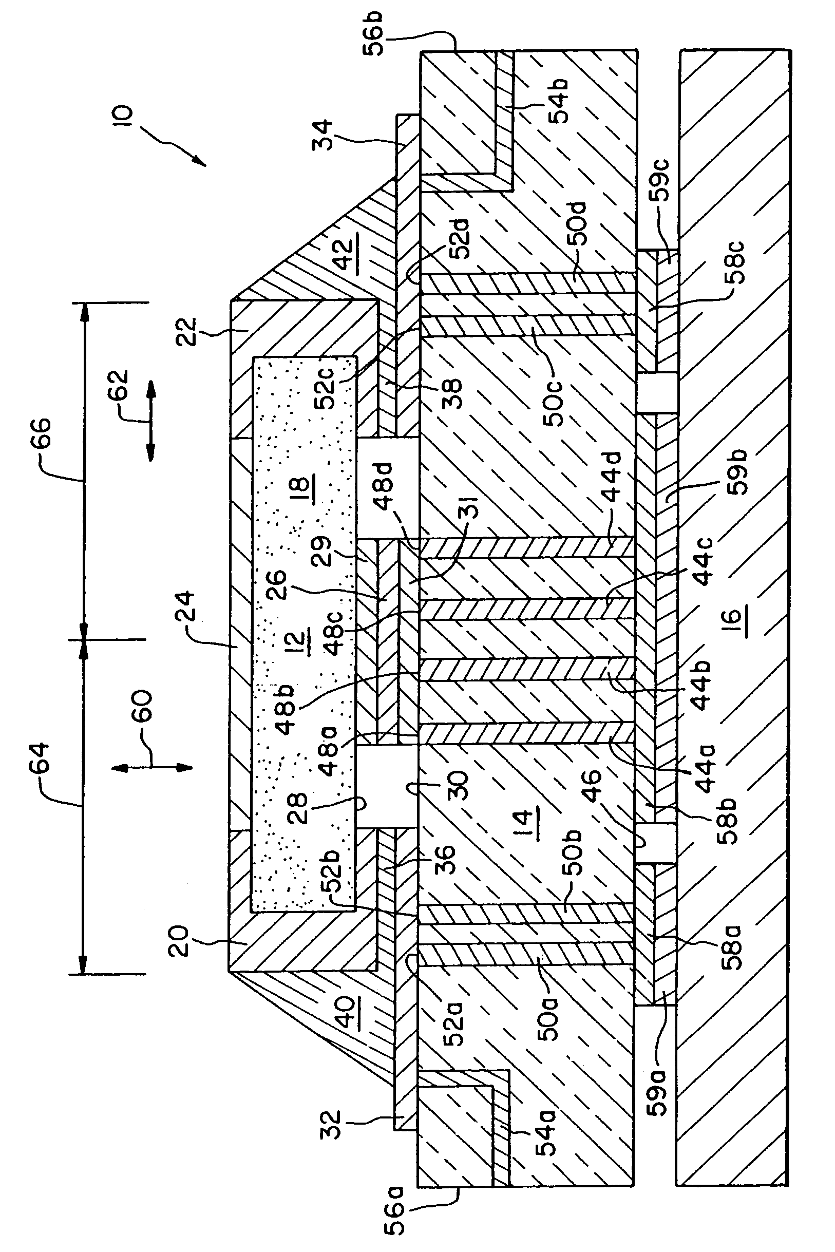
[0014]One embodiment of an electronic component arrangement 10 of the present invention is shown in the drawing. Arrangement 10 includes a discrete electronic component in the form of a printed ink chip resistor 12 mounted on a substrate in the form of a printed circuit board (PCB) 14. A heat sink 16 absorbs and dissipates heat from PCB 14.

[0015]Chip 12 includes a body 18, a first terminal 20, a second terminal 22 and a centre-exposed pad 29. Body 18 may be formed of a ceramic material, for example, while terminals 20, 22 and pad 29 may be formed of an electrically conductive metal. In the embodiment shown, chip 12 is in the form of a printed ink resistor or polymer thick film (PTF) resistor having a layer of in...


PUM


Abstract

An electronic component arrangement includes a discrete electronic component having first and second terminals and a centre-exposed pad. A substrate has a first electrical conductor electrically connected to the first terminal, a second electrical conductor electrically connected to the second terminal, and a third electrical conductor. A thermally conductive element is in direct thermal communication with both the centre-exposed pad of the electronic component and the third electrical conductor of the substrate.

Description

BACKGROUND OF THE INVENTION[0001]Discrete electronic components in the form of surface mounted devices and passive chip components are widely used in the electronics industry. Such components may be formed of ceramic, for example. In many applications, the components carry a large power load in relation to the components' size. The high power density requirements may result in premature failure of the components due to heat stress and thermal expansion. For example, repeated thermal expansion may cause cracking in the solder joints at the terminals of the components, as well as oxidation and intergranular corrosion.[0002]A typical power rating of a ceramic resistor chip, such as a model 2512 chip, is less than or equal to one watt per chip from room temperature up to 70° C. However, above 70° C. the power rating steadily falls to 0 watt at about 155° C. Temperature cycling testing reveals that such chips cannot pass a test including 1000 cycles between −40° C. aid 150° C. Many autom...

Claims


Application Information

Patent Timeline
Patent Type & Authority Patents(United States)
IPC IPC(8): H05K7/10H01L23/48H05K1/18H05K5/02
CPCH05K1/0206H05K3/3442H05K2201/066H05K2201/10636H05K2201/10969Y02P70/50
Inventor NAH, CHIH KAISTILLABOWER, MORRIS DPAN, BINGHUAYONG, SIM YINGGROMALA, PRZEMYSLAW
Owner DELPHI TECH IP LTD
Why Eureka
Try Eureka