Ferroelectric capacitor and semiconductor device having a ferroelectric capacitor

a technology of ferroelectric capacitor and ferroelectric capacitor, which is applied in the direction of capacitors, solid-state devices, transistors, etc., can solve the problems of ferroelectric layer, damaged layer on the side surface, and inability to normal operation of ferroelectric capacitors, so as to reduce the influence of damaged layer

Inactive Publication Date: 2006-12-19
LAPIS SEMICON CO LTD
View PDF9 Cites 3 Cited by
  • Summary
  • Abstract
  • Description
  • Claims
  • Application Information

AI Technical Summary

Benefits of technology

[0013]Accordingly, in one aspect of the present invention, a ferroelectric capacitor for reducing an influence of a damaged layer is provided. The ferroelectric capacitor includes a bottom electrode which has a projecting portion, a top electrode, a ferroelectric layer and a dielectric layer formed between the bottom electrode and the top electrode. The dielectric layer is formed on a peripheral area of the bottom electrode. The ferroelectric layer is formed on the dielectric layer and on the projecting portion of the bottom electrode.

Problems solved by technology

However, a damaged layer might be formed on a side surface of the ferroelectric layer.
If a damaged layer is formed, normal operation of the ferroelectric capacitor might be inhibited and reliability of the ferroelectric capacitor might not be ensured.
However, an amount of remaining polarization is not increased after the cleaning.
Such process therefore is not an effective solution.

Method used


Image

  • Ferroelectric capacitor and semiconductor device having a ferroelectric capacitor
  • Ferroelectric capacitor and semiconductor device having a ferroelectric capacitor
  • Ferroelectric capacitor and semiconductor device having a ferroelectric capacitor

Examples


first preferred embodiment

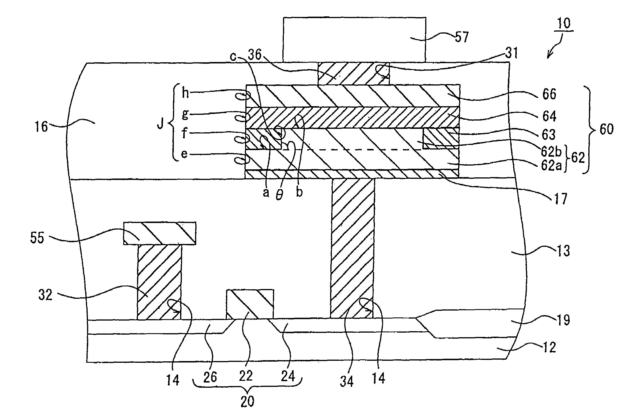
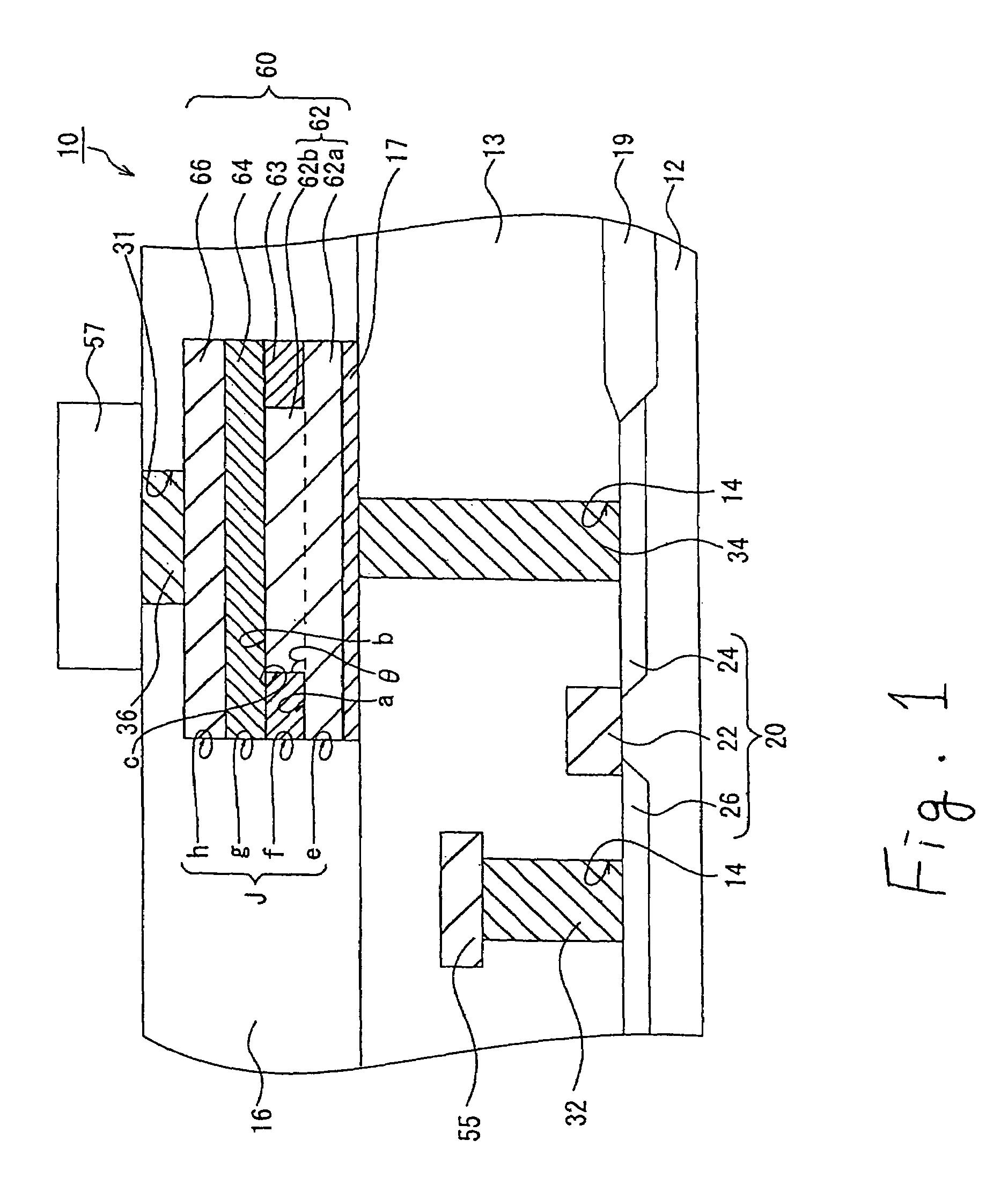
[0028]FIG. 1 is a cross-sectional view showing a semiconductor device 10 of a first embodiment of the present invention. The semiconductor device 10 as shown in FIG. 1 is a cross-sectional view taken along line 1–1′ in FIG. 2. In this embodiment, a stack type FeRAM is described.

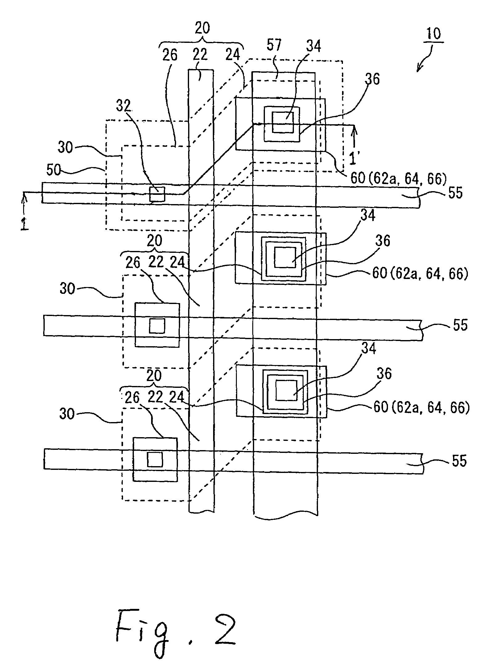
[0029]Initially, the semiconductor device 10 is explained in reference to FIG. 2. A memory cell 50 of the semiconductor device 10 includes a MOSFET(Metal Oxide Semiconductor Field Effect Transistor) 20 and a ferroelectric capacitor 60 as shown in FIG. 2. The transistor 20 includes a source region as a first region 24 and a drain region as a second region 26 and a gate electrode as a control electrode 22. The first region 24 and the second region 26 are formed in an active area 30 and the gate electrode 22 is arranged on an area which is located between the first region 24 and the second region 26. The gate electrode 22 is used as a word line in the semiconductor device 10. The drain region 26 is connected to ...

second preferred embodiment

[0065]In the second embodiment, a projection portion 72a of a bottom electrode 72 and a plate portion 72b of the bottom electrode 72 are made of different material as shown in FIG. 6.

[0066]In this embodiment, the bottom electrode 72 of a ferroelectric capacitor 70 includes the plate portion 72a such as iridium and the projection portion 72b such as iridium oxide.

[0067]Next, a method of fabricating a semiconductor device 200 is explained in reference with FIGS. 7(A)–7(C).

[0068]From the step for forming the transistor 20 to the step for forming plug 34 are performed as described in the first embodiment.

[0069]Then, the iridium layer 71 which has 100 nm thickness is formed on the barrier metal 17 by a sputtering technique. Then, the iridium oxide layer 73 which has 100 nm thickness is formed on the iridium layer 71 by a reactive sputtering technique as shown in FIG. 7(A). The iridium layer 71 and the iridium oxide layer 73 form a conductive layer 74 for forming the bottom electrode.

[007...

third preferred embodiment

[0074]FIG. 8 is a cross-sectional view showing a semiconductor device 300 of a third embodiment of the present invention. FIGS. 9(A) to (C) are views showing manufacturing steps for a semiconductor device 300 of the third embodiment of the present invention.

[0075]The bottom electrode 82 includes a stacked plate portion 82a and a projection portion 82b such as platinum formed on the stacked plate portion 82a. The stacked plate portion 82a includes an iridium layer 821 as a lower layer and an iridium oxide layer 822 as an upper layer.

[0076]The iridium oxide layer 822 has good adhesive characteristic for adhering to the platinum projection portion 82b. The iridium layer 821 has a function for resisting oxidation. As a result, an end point of etching for forming the projection portion 82b is found easily, and the platinum projection portion 82b can be used. That is, the platinum projection portion 82b which improves a capacitor characteristic and the iridium layer 821 can be used as the...


PUM

PropertyMeasurementUnit
angleaaaaaaaaaa
thicknessaaaaaaaaaa
thicknessaaaaaaaaaa

Abstract

A ferroelectric capacitor including a bottom electrode which has a projecting portion, a top electrode, a ferroelectric layer and a dielectric layer formed between the bottom electrode and the top electrode. The dielectric layer is formed on a peripheral area of the bottom electrode. The ferroelectric layer is formed on the dielectric layer and on the projecting portion of the bottom electrode. As a result, a damaged layer which is formed during an etching process occurs at the ineffective area of the ferroelectric capacitor.

Description

CROSS REFERENCE TO RELATED APPLICATION[0001]A claim of priority under 35 U.S.C. §119 is made to Japanese Patent Application No. 2003-024772, filed Jan. 31, 2003, which is herein incorporated by reference in its entirety for all purposes.BACKGROUND OF THE INVENTION[0002]1. Field of the Invention[0003]The present invention relates to a ferroelectric capacitor and a semiconductor device having a ferroelectric capacitor.[0004]2. Description of the Related Art[0005]A FeRAM(ferroelectric random access memory) uses a ferroelectric capacitor. Data can be read quickly from the FeRAM, which can be operated to provide random access. Therefore, the FeRAM is expected as a new type of nonvolatile memory.[0006]A memory cell of the FeRAM includes a switching transistor and a ferroelectric capacitor. The FeRAM uses a function of the ferroelectric layer for reversing an electric field by an intrinsic polarization and for retaining the electric field.[0007]The FeRAM is classified broadly into either a...

Claims


Application Information

Patent Timeline
Patent Type & Authority Patents(United States)
IPC IPC(8): H01L29/76H01L29/94H01L31/062H01L31/113H01L31/119H01L27/105H01L21/02H01L21/8246H01L27/115H01L27/11507
CPCH01L27/11502H01L27/11507H01L28/75H01L28/55H10B53/30H10B53/00
Inventor ITO, TOSHIO
Owner LAPIS SEMICON CO LTD
Why Eureka
Try Eureka