Semiconductor apparatus

a technology of semiconductor and apparatus, which is applied in the direction of valve operating means/release devices, pulse generators, pulse techniques, etc., can solve the problems of deterioration in efficiency, delay time, and relatively large delay time of mos-type devices, and achieves stable operation of mos-type devices, simple configuration, and improved response and efficiency.

Active Publication Date: 2006-12-19
MITSUBISHI ELECTRIC CORP
View PDF12 Cites 32 Cited by
  • Summary
  • Abstract
  • Description
  • Claims
  • Application Information

AI Technical Summary

Benefits of technology

[0010]In view of the above circumstances, it is an object of the present invention to provide a semiconductor apparatus capable of stably operating a MOS-type device using a relatively simple configuration while facilitating improvement in response and efficiency, and reduction in EMI noise and switching loss.
[0012]According to the present invention, in the gate turn-on operation, the gate current is increased only for the first predetermined time by turning on the first switch and turning on the third switch for the first predetermined time. Thus, the time-period allowing the gate to be turned on can be reduced. In the gate turn-off operation, the discharge current from the gate is increased only for the second predetermined time by turning on the second switch and turning on the fourth switch for the second predetermined time. Thus, the time-period allowing the gate to be turned off can be reduced. The semiconductor apparatus constructed as above can achieve reduction in switching loss and delay time.

Problems solved by technology

In a semiconductor apparatus having a tail-end circuit with a MOS-type device to be driven by an external signal, the MOS-type device has a relatively large delay time between the receiving of the external signal intended to turn off the device and the establishment of its actual OFF state.
This delay time is caused by a capacitance around the gate of the device.
Thus, the technique of controlling the gate charging and discharging times of the device only by a gate resistor set at a certain fixed value results in creation of another delay time in addition to the delay time due to the threshold voltage of the device, which leads to deterioration in efficiency.
Otherwise, if the switching speed during the turn-on is lowered to reduce EMI noise, a switching loss will be increased.
As above, there is a trade-off relationship between EMI noise and switching loss.
Further, the circuit involves a number of switches and a complicate control for sequentially turning on the switches depending on the characteristics of the IGBT.
In the circuit disclosed in Patent Publication 2, if the gate resistance is sharply changed during a turn-on operation where a collector current flows at a value approximately equal to a comparison reference value of the comparator, the operation of the IGBT is likely to become unstable to cause oscillation in an output current therefrom.

Method used


Image

  • Semiconductor apparatus
  • Semiconductor apparatus
  • Semiconductor apparatus

Examples


first embodiment

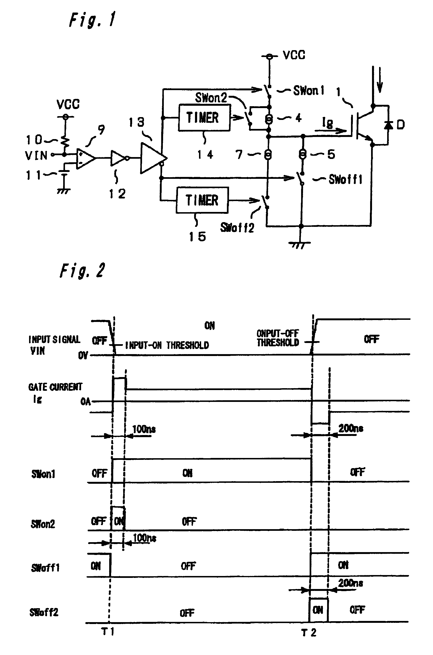
[0019][First Embodiment]

[0020]FIG. 1 shows a MOS-type power device and a drive system thereof in a tail-end circuit of a semiconductor apparatus according to a first embodiment of the present invention. For turning on the gate a power device (e.g. IGBT) 1 associated with a freewheel diode D, two switches SWon 1, SWon 2 (or first and third switches) each composed of a transistor are inserted in series between a power supply VCC and the gate of the power device 1. A constant current device 4 is connected in parallel with the switch SWon 2.

[0021]For turning off the gate of the power device 1, a switch SWoff 1 (or second switch) composed of a transistor is connected between the gate and emitter of the power device 1 through a constant current device 5, and a switch SWoff 2 (or fourth switch) composed of a transistor is connected between the gate and emitter of the power device 1 through a constant current device 7.

[0022]An input signal VIN is entered into a positive input terminal of a ...

second embodiment

[0032][Second Embodiment]

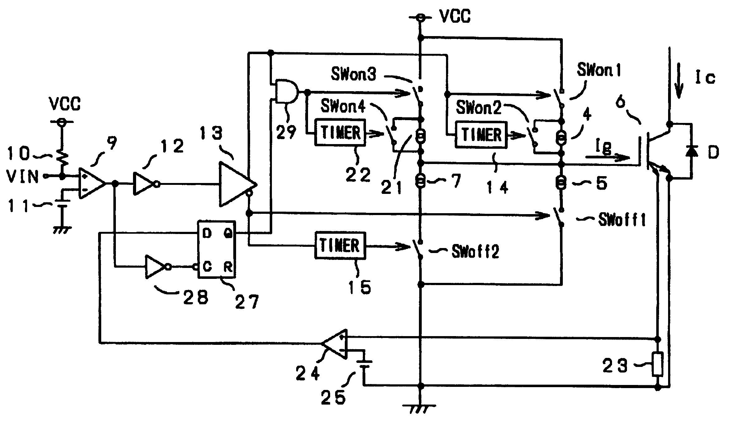
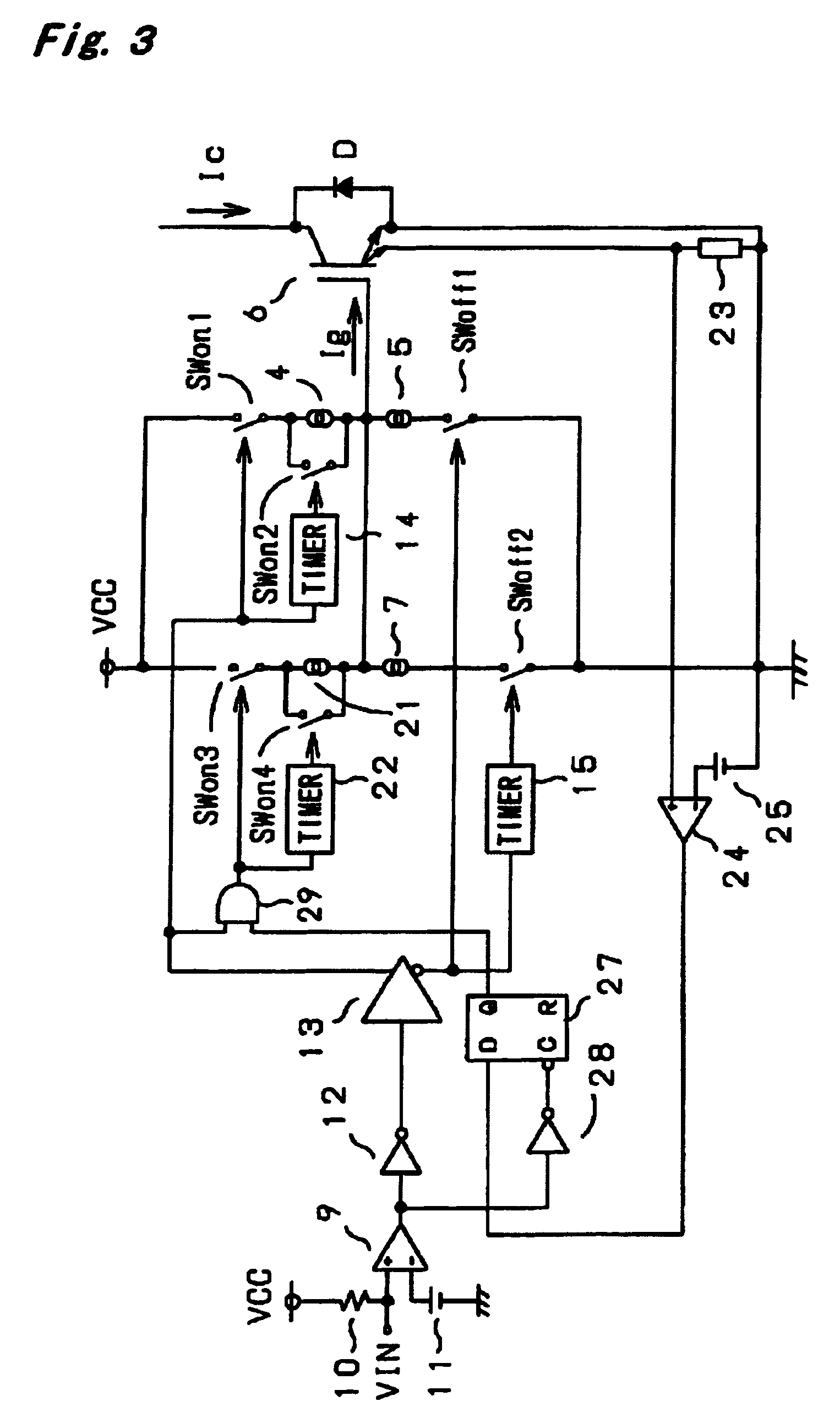
[0033]A second embodiment of the present invention is configured such that in accordance with the amount of the current flowing through an IGBT turned on according to a first turn-on operation, a gate charge current in a second turn-on operation subsequent to the first turn-on operation is varied to change a switching speed during turn-on of the gate. FIG. 3 shows a tail-end circuit of a semiconductor apparatus according to the second embodiment.

[0034]In the circuit of FIG. 3, the same component or element as that in FIG. 1 is defined by the same reference numeral or code. As shown in FIG. 3, in addition to a turn-on circuit comprised of a switch SWon 1, a switch SWon 2, a constant current device 4 and a timer 14, the circuit additionally includes a switch SWon 3, a switch SWon 4, a constant current device 21 and a timer 22, as a second turn-on circuit. The following circuits are added in order to control this 2nd turn-on circuit.

[0035]An IGBT 6 has a second...


PUM


Abstract

Disclosed is a semiconductor apparatus having an IGBT, which includes a switch SWon 1 for supplying a gate current during an operation for turning on the gate of the IGBT, a switch SWoff 1 for discharging a gate capacitance during an operation for turning off the gate, a switch SWon 2 for increasing the gate current, a timer 14 for turning on the switch SWon 2 in conjunction with the turn-on of the switch SWon 1 and then maintaining the turn-on of the switch SWon 2 only for a first predetermined time, a switch SWoff 2 for increasing the discharge current during the gate turn-off operation, and a timer 15 for turning on the switch SWoff 2 in conjunction with the turn-on of the switch SWoff 1 and then maintaining the turn-on of the switch SWoff 2 only for a second predetermined time.

Description

BACKGROUND OF THE INVENTION[0001]The present invention relates to a semiconductor apparatus using an MOS-type device, designed to control a time-period between the receiving of an external signal and the actual action of the device itself so as to achieve improvement in response and efficiency, and reduction in EMI noise and switching loss.[0002]In a semiconductor apparatus having a tail-end circuit with a MOS-type device to be driven by an external signal, the MOS-type device has a relatively large delay time between the receiving of the external signal intended to turn off the device and the establishment of its actual OFF state. This delay time is caused by a capacitance around the gate of the device. Heretofore, in a circuit for switching the gate, a resistor inserted in series to the gate has been preset at a certain value to adequately control the charge and discharge of the gate. That is, the rise and fall times of a gate voltage have been adjusted in accordance with a CR tim...

Claims


Application Information

Patent Timeline
Patent Type & Authority Patents(United States)
IPC IPC(8): H03K17/687H02M1/08H01L29/74H03K17/04H03K17/0412H03K17/06H03K17/16H03K17/56H03K19/00H03K19/01
CPCH03K17/0406H03K17/164H03K17/167H03K17/04123H03K17/04206F16K25/00F16K31/06
Inventor INOUE, TAKAHIRO
Owner MITSUBISHI ELECTRIC CORP
Why Eureka
Try Eureka