Eureka AIR delivers breakthrough ideas for toughest innovation challenges, trusted by R&D personnel around the world.

Spin etcher with thickness measuring system

Active Publication Date: 2006-12-26
SEMES CO LTD
View PDF17 Cites 1 Cited by
  • Summary
  • Abstract
  • Description
  • Claims
  • Application Information

AI Technical Summary

Benefits of technology

[0006]According to the present invention, the thickness measuring system includes a plurality of optical probes, a light source unit, a detector, and a thickness measuring controller. The optical probes are located over the substrate, and allow a light to impinge on the substrate surface and sense the reflected light. The light source unit supplies a light of a specific wavelength to the respective optical probes. The detector detects an interference signal of the reflected light transmitted from the respective optical probes. The thickness measuring controller estimates the interference signal detected from the detector to measure a thickness and transfers data on the measured thickness to the main controller. The optical probes are installed in a probe folder to prevent the etchant from corroding them.

Problems solved by technology

In this case, an etching amount error may occur due to variations in etchant concentration and variations in process conditions.
The etching amount error makes it difficult to exactly adjust an etching thickness.

Method used


Image

  • Spin etcher with thickness measuring system
  • Spin etcher with thickness measuring system
  • Spin etcher with thickness measuring system

Examples


Embodiment Construction

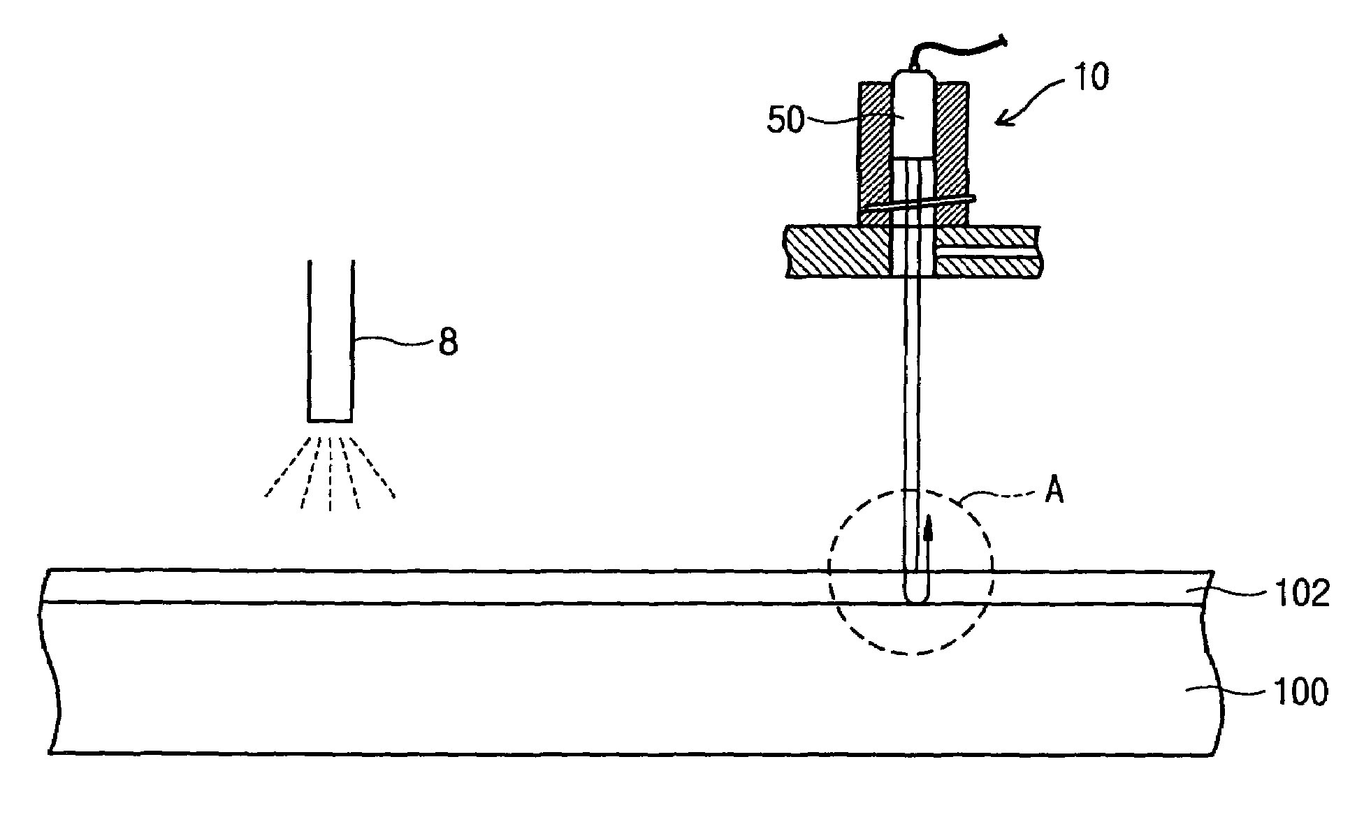
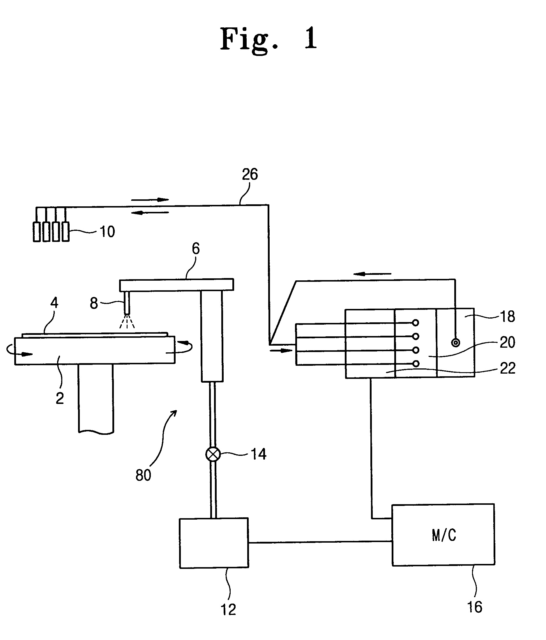
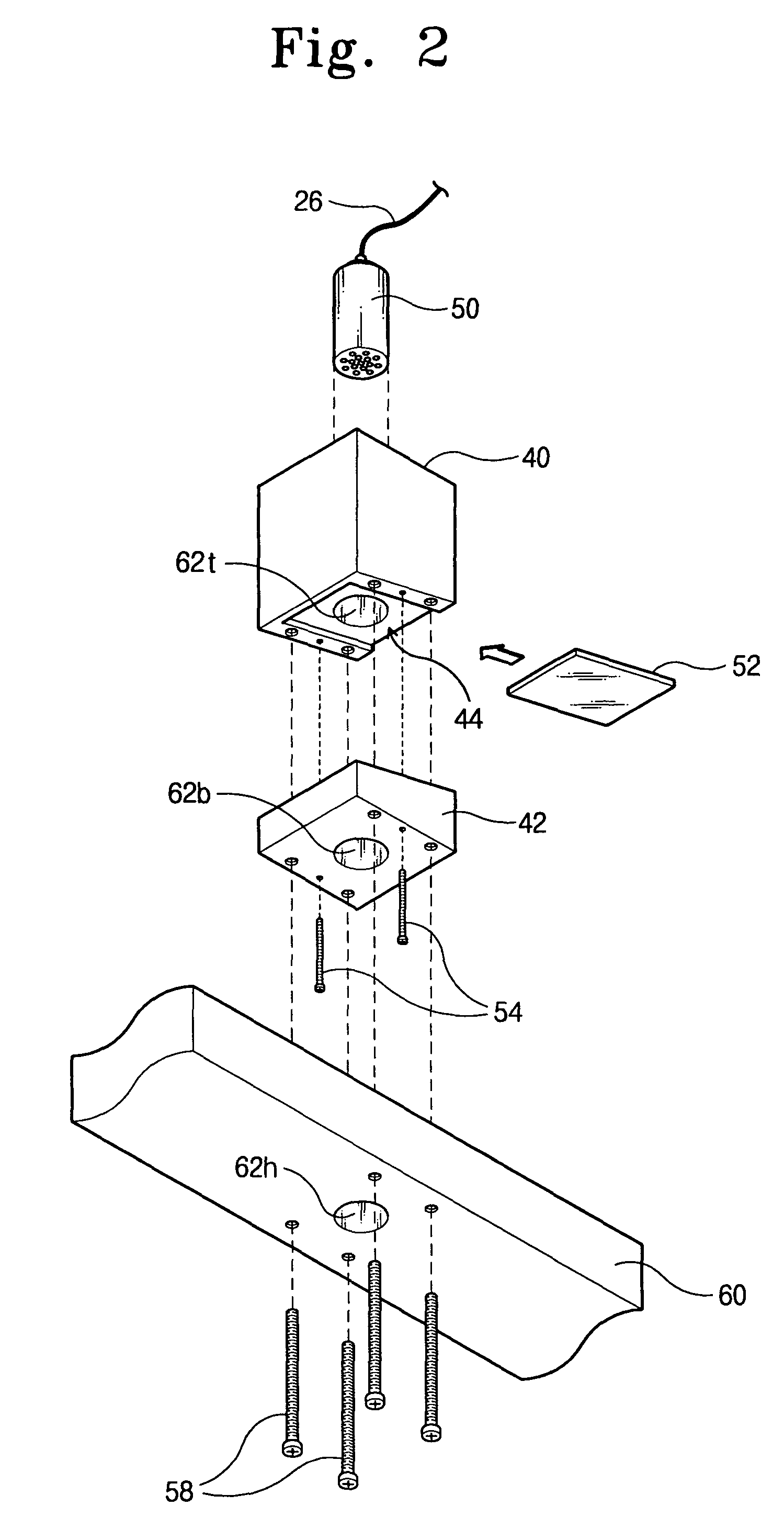
[0012]Referring to FIG. 1, a spin etcher according to the present invention includes a spin head 2, an etchant supply means 80, and a thickness measuring system. A substrate 4 is located on the spin head 2. The spin head 2 is fixed to a rotatable shaft to rotate at a constant speed. The thickness measuring system has an optical probe unit 10, a light source unit 18, a detector 20, and a thickness measuring controller 22. The optical probe unit 10 is installed apart from an upper side of the substrate 10 as far as a predetermined distance, and has a light section for emitting a light and a light receiving section for receiving a light reflected from a substrate. The light source unit 18 produces a short-wavelength light using an ultraviolet lamp or a Xenon lamp, and transmits the short-wavelength light to the light section of the optical probe unit 10. The detector 20 serves to remove noise of the light transmitted from the light receiving section of the optical probe unit 10 and to ...


PUM

PropertyMeasurementUnit
Timeaaaaaaaaaa
Timeaaaaaaaaaa
Angleaaaaaaaaaa

Abstract

A spin etcher with a thickness measuring system includes a rotatable spin head, etchant supply means, and etchant supply controller. A substrate is mounted upon the spin head. The etchant supply means is disposed over the substrate, and sprays an etchant onto the substrate. The etchant supply controller controls the etchant supply. The spin etcher further includes a main controller for transferring an etchant supply stop signal to the thickness measuring system and the etchant supply controller. The thickness measuring system allows a light to impinge on a surface of the substrate, and analyzes an interference signal of the light reflected from the substrate to measure a thickness of a thin film. The main controller compares a result measured by the thickness measuring system with a reference value, and transfers the etchant supply stop signal to the etchant supply controller before the measured result reaches the reference value. During a predetermined time after the etchant supply is stopped, the thin film is etched one more time by an etchant remaining on the substrate. As a result, the thickness of the thin film reaches the reference value.

Description

FIELD OF THE INVENTION[0001]The present invention relates to equipment for fabricating semiconductor devices and, more particularly, to a spin etcher for etching a specific layer by spraying an etchant onto a substrate mounted on a rotating spin head.BACKGROUND OF THE INVENTION[0002]Generally, semiconductor devices are fabricated by means of complex processes such as deposition processes where thin films are deposited on a substrate, photolithographic processes where photoresist patterns are formed on the substrate, ion implantation processes where impurities are implanted into the substrate, and etching processes where specific layers are removed. The etching process may include a dry etching process and a wet etching process. In the dry etching process, plasma is produced in a vacuum chamber to remove a thin film formed on a substrate surface. In the wet etching process, a substrate is submerged into a chemical bath to remove a thin film. A spin etcher was recently introduced, in ...

Claims


Application Information

Patent Timeline
IPC IPC(8): G01B11/02H01L21/3063C23F1/08G01B11/06H01L21/306H01L21/66
CPCG01B11/0625H01L22/12H01L21/3063
Inventor KIM, CHUNG-SIKBAE, JEONG-YONG
Owner SEMES CO LTD
Why Eureka
Eureka Blog
Learn More