Method for producing a high resolution detector array

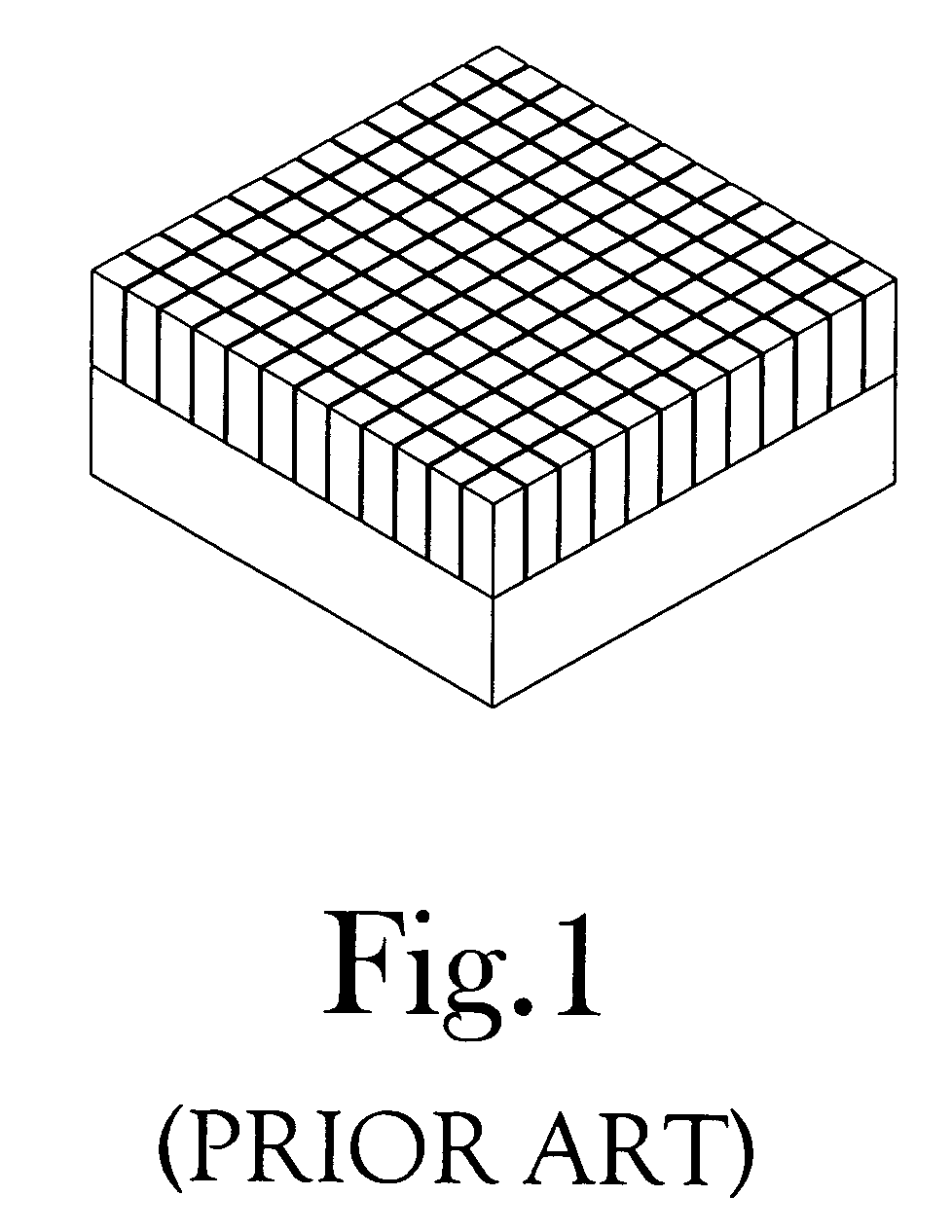
a detector array and high-resolution technology, applied in the field of high-resolution detector array production, can solve the problems of inability to produce arrays of individual crystals, inability to produce individual crystal arrays, time-consuming and difficult to consistently do hand wrapping individual crystals, etc., to achieve enhanced fabrication methods

Inactive Publication Date: 2007-01-02
SIEMENS MEDICAL SOLUTIONS USA INC
View PDF9 Cites 38 Cited by
  • Summary
  • Abstract
  • Description
  • Claims
  • Application Information

AI Technical Summary

Benefits of technology

[0009]In one embodiment of the present invention, the fabrication methodology is enhanced by handling scintillator bars rather than single crystals when gluing on the optical film as well as polishing the scintillator bars. Namely, a scintillator boule is cut into bars of a selected dimension, for example 30 mm wide, which then maybe polished. A selected number, N, of these scintillator bars can then be glued together with sheets of an optical film sandwiched between each bar (coating the scintillator bars and optical sheets with an optical adhesive). Suitable optical films include mono-layer or multi-layer, nonwettable reflective films such as polyester films and polyethylene films, including Polyethylene...

Problems solved by technology

However, this method is not feasible for producing arrays of individual crystals.
However, plumbers Teflon® tape is not a realistic choice for large cameras and/or cameras that use very small crystals.
Further, hand wrapping individual crystals is both time consuming and difficult to do consistently.
Hand wrapping with Teflon® tape also limits the reduction of crystal size for future cameras.
In addition, plumbers Teflon® tape, or thicker 8 mil Teflon® tape, is not an idea...

Method used


Image

  • Method for producing a high resolution detector array
  • Method for producing a high resolution detector array
  • Method for producing a high resolution detector array

Examples


Embodiment Construction

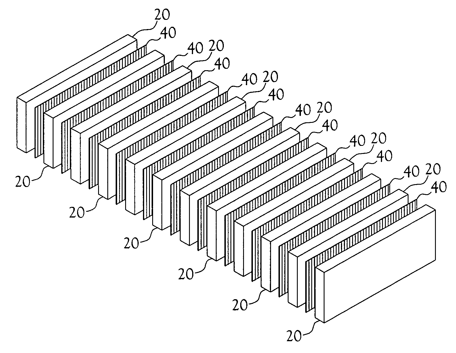
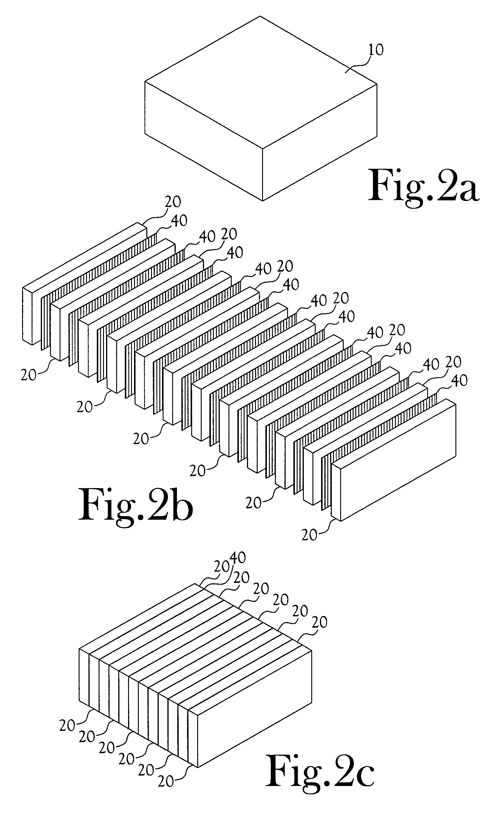
[0020]The detector designs produced by the method disclosed herein, along with its alternate embodiments, will enable finer spatial resolution than is achievable with current state of the art detector fabrication methodologies. The method can be utilized to produce a detector array comprised of a single scintillator material, or as described herein, can employ the use of two or more scintillator materials of different decay times. The decay times are used as one of the parameters in determining the scintillator elements loci in position space. Most current detector designs use the decay time for depth of interaction encoding (DOI). Variants of the new design would also be capable of providing this feature.

[0021]In general, the detector fabrication method will provide very high packing fraction i.e. the distance between scintillator elements will be minimized so the detector efficiency will be higher than is currently achievable. Another important feature of the design is that four t...


PUM

PropertyMeasurementUnit
Lengthaaaaaaaaaa
Timeaaaaaaaaaa
Decay rateaaaaaaaaaa

Abstract

A method for producing a high resolution detector array so as to provide very high packing fraction, i.e. the distance between scintillator elements is minimized so the detector efficiency will be higher than is currently achievable. In the preferred embodiment of the present invention, the fabrication methodology is enhanced by handling scintillator bars rather than single crystals when gluing on an optical film as well as polishing the scintillator. Namely, a scintillator boule is cut into wide bars of a selected dimension, for example 30 mm, which are then acid etched or mechanically polished. A selected number, N, of these scintillator bars can then be glued together with sheets of optical film between each bar (coating the scintillator disks and optical film with an adhesive of a selected index of refraction). The glued bar block is then cut again into bars in a perpendicular direction, and these new scintillator-optical film bars are polished. Finally, a selected number, M, of these scintillator-optical film bars are glued together with sheets of optical film between each bar; thus creating a polished N×M scintillator-optical film array, (where M may or may not be equal to N), without having to handle individual scintillator crystals or small pieces of optical film.

Description

CROSS-REFERENCE TO RELATED APPLICATIONS[0001]This is a continuation-in-part application that claims the benefit of the filing date of Non-Provisional patent application Ser. No. 09 / 972,339 filed on Oct. 5, 2001 now U.S. Pat. No. 6,749,761.STATEMENT REGARDING FEDERALLY SPONSORED RESEARCH OR DEVELOPMENT[0002]Not ApplicableBACKGROUND OF THE INVENTION[0003]1. Field of Invention[0004]This invention pertains to a method of producing a scintillator detector array that may be used in various applications, such as, but not limited to, a positron emission tomography detector module or nuclear physics applications. More specifically, it relates to a method of producing a high resolution detector array that can be coupled to photodetectors. In certain applications, the photodetector provides an accurate timing pulse and initial energy discrimination, identification of the crystal interaction, which may include the depth of interaction (DOI).[0005]2. Description of the Related Art[0006]When cons...

Claims


Application Information

Patent Timeline
IPC IPC(8): B29D11/00
CPCG01T1/202B29D11/0074
Inventor ANDREACO, MARK S.WILLIAMS, CHARLES W.MOYERS, J. CLIFTONVAIGNEUR, KEITH
Owner SIEMENS MEDICAL SOLUTIONS USA INC
Why Eureka
Try Eureka